Frequently Asked Questions
Live Q&A

ZofzPCB Users' Forum
FAQ - Table of Contents
- How to export IPC-356 File?
- How to load Gerber files set, using Auto files assignment?
- What are .camset and .zofzproj files?
- Missing tracks, transparent PCB volume, missing PCB outline
- Can ZofzPCB display µVias, Buried Vias and Blind Vias?
- How to handle the Excellon Warning: drill plate 1 - unknown tools?
- How to reduce momentary freezing in Windows caused by ZofzPCB display?
- How to reduce the load of the GPU?
- Why am I not allowed to overwrite component selection, even if the models are there?
- How to load the license key?
How to export IPC-356 File?
Warning: Component Reference text length

The IPC-356 allows for reference text length up to 6 characters. For example, the reference text "BTN_DOWN" is truncated to "BTN_DN". (Eagle could have been allowing for one more character, btw.) Pay attention that the truncated names are not overlapping after all truncations.
Truncated components' references will not match respective references in the BOM file, making it challenging to auto-detect the BOM columns.
Very oddly, the IPC-356 format is a fixed-width format. Therefore, there is a possibility of a net name aliasing by IPC-356 specification.
The original name is renamed to a short alias, used within IPC-356. There is no such option for the component reference, however.
I have found out that some other ecad programs do not bother and export longer designators without warning. That approach is readable,
under the condition that the reference name does not contain a minus sign, as the format forces "-" after the reference field.
This approach might be problematic to some parsers, however. Another solution would be not allowing for component designator
lengths above 6 characters already on the input (schematic) side.
The IPC-356 expects designators to be like "SW1", see Wikipedia
And sticking to the familiar names makes it easier for ZofzPCB to assign more accurate component models.
-
How to export IPC-356 File from Eagle?
Drop Down Menu: File / Export / IPC
See the following Eagle UI screenshot:
-
How to export IPC-356 File from Kicad?
Drop Down Menu: File / Fabrication Outputs / IPC-D-365 Netlist File...
See the following KiCad UI screenshot:
-
How to export IPC-356 File from Protel99se?
- Drop Down Menu: Tools / CAM Wizard...
- In Output Wizard: Select "Test Points", click "Next"
- In Output Wizard: Select "IPC-D-365A", deselect all other, if you do not need it, click "Next"

-
How to export IPC-356 File from CirCAD?
Original exported IPC-356 file is missing holes/pads having no assigned net-name or pin-name.
Please use provided command-line tool to extract the IPC-356 file directly from the CirCAD PCB file.Usage:
CirCAD2ipc test.pcb
The program creates test.ipc file, possibly overwriting any existing file!
For additional security, please check the downloaded file signature.Download CirCAD2ipc.exe
How to load Gerber files set, using Auto files assignment?
As I have some feedback about problems reading Eagle Gerbers, I have installed Eagle 9.4.2 free version.
I took an Open Hardware project: hackaday/BoborBuino
There is my walk-through.
- I started by exporting the CAM files. The Gerber export results are saved in multiple directories, named: Assembly DrillFiles, GerberFiles.
This is not standard, and it is not compatible with ZofzPCB Auto-Detection. No problem to move the files to a single directory, though. - Automatic recognition composition of files: "drill_1_16.xln" was not recognized as a drill file. - I have fixed the "CAM_Load_Rules.txt" mask file immediately. (available by next release)
- Now press the [Auto Load] button.

- Now press the [OK: Read & Render] button.

- Board outline:
The board outline is in a separate file - good.
ZofzPCB does not read it correctly, missing the PCB milling division of the 2 boards (top/bottom). What is so complicated in the board outline?
What we need is a clear cut line, as it would guide the tool.
I have checked the drawing in a 2D Gerber viewer (gerbv). The viewer is just displaying the line drawing instead of attempting to convert it to a "solid" polygon, of course.

I have removed those overlapping arcs, forming the circles (holes), knowing that they are repeated as drills.
Obviously, my algorithm could not convert the overlapped arcs to single circles and quit before finishing the whole drawing. (edit: Version 2.0 features a better algorithm.)
I could smell the problem by seeing the Gerber file size of the outline being 111KB vs e.g. copper-top 40KB. I know it will be difficult for me.
Indeed, there is much more information in the copper layer than in the board outline, but the file size says the opposite.
Anyway, I consider it as a zofzpcb bug. (Edit: Fixed)
Another point - the standard size of a cut-out milling tool is 2.5 mm in diameter. Possibly this can be changed, but not to zero, to accomplish a rectangular cut-out. Inner cut-outs will be quietly adjusted - to having a specific radius "stadium" curve.
This is not critical, but it will be edited by the cam operator the way he wishes. - I have repeated the above steps. I was lucky - my guess was correct.
- Rendering
The silkscreen renders for hours! It is a ZofzPCB old bug. (edit: Version 2.0 features a better algorithm.)
Again - the silkscreen_top is 220KB (vs. copper-top 40KB.) I am giving it another try - this time using the Imperial scale. Magically it takes only one second to render. And the size of all imperial Gerbers is about half the size of their metrics versions. Why?

-
IPC netlist vs. Copper netlist errors:
as the above error dialog shows, there is one short connection.
Looking closer using menu Netlist / Errors

It seems that the ring around the speaker holes was added without an accompanying schematic entry or so. This kind of problem is cosmetic. -
I have the components display:

There are some differences between what ZofzPCB have shown and what the project's photos show. Some problems are the lack of proper models, some other (adjustable), - wrong detection, primarily because of non-standard reference naming. Right-click model menu lets resolve some of the problems, either by removing the component or selecting a different model, or changing some parameter's value.

-
The final view - do not forget to save the .camset file and/or the rendered board mesh data.

Check out the rendered project on The Project Gallery
What are .camset and .zofzproj files?
What is .camset file?
Preparing Gerber files set for display in ZofzPCB requires some work. The .camset file contains all the configurations created in the setup process so that you can read the Gerber files quickly for a second time. Example: after applying changes in the ECAD program and regenerating the Gerber files. If you open the saved .camset file, ZofzPCB will also read all the CAM files and render (flatten) the PCB model again.
- Stackup and list of all layers. For each layer:
- File Name
- Type - e.g., copper, silkscreen, core, etc
- Thickness, etc
- The board outline is a part of the stackup list. The thickness of the board outline is the thickness of the whole PCB
- List of drill files. For each drill file:
- File Name
- Span (thru, or from-to copper numbers)
- Platting type, micro-via options
- IPC-356 and BOM file names
- List of user defined layer types, like glue, gold or carbon
- Settings of Gerber and drill file parser, for older on incomplete headers, missing information like polarity
- Color settings:
- For each layer in the stackup
- For each layer type
- Netlist color schema
- Netlist color exceptions (manual adjustments)
- Color mixer settings
- Components:
- Result of automatic and manual component model selection, model parameters
- Body Builder model data
- Saved camera positions 0..9
What is .zofzproj file?
The file contains all internal data structures the program needed to display and browse the PCBA. The file also includes all the information the .camset file contains. Reading the .zofzproj file leads to a direct display of the PCBA model without the flattening and triangulation phase. Gerber and other CAM files are no longer needed.
- The file is compressed and encrypted
- The "Read Only" option:
- The file contains encrypted access flags and may miss specific information
- PCBA model is displayed in premium mode by a software/user without the premium license
- You need the premium license to create the "Read Only" file
Missing tracks, transparent PCB volume, missing PCB outline
Sometimes PCB renders in a wired way, strange gradient effects appear, PCB volume is transparent, tracks are partially missing.
Those are typical symptoms of the misinterpreted board outline.
The Gerber primary data are often accompanied by text, symbols, frames e.t.c. not representing
the PCB structures but carrying descriptions targeting the manufacturer.
These parts of the image must be removed before a 3D model of the board is created.
Typically ZofzPCB uses the Board Outline drawing to decide what regions of the image must be preserved and what regions are to be removed.
If the detection of the board outline fails, yielding e.g. a small object placed inside (or worst) outside the board,
those strange artifacts may be present.
Please check the following:
- The Board Outline Layer must be present in the stackup if the file is available.
- ZofzPCB can extract the outline drawing from a copper or silkscreen, if it is distinguishable from other elements, by a track thickness below some threshold. All other track objects must have their thickness value above the threshold. See "Meta Drawing" settings.
- The board outline drawing must be made out of continuously overlapping tracks segments (straight or arcs).
- As the description text characters may also form closed-loop track areas, please select a way to identify the outline in "How To Identify" settings.
Can ZofzPCB display µVias, Buried Vias and Blind Vias?
The Laser Via drill files are detected automatically, based on the via sizes, ratio, etc. You can also set these attributes manually.
See the stackup dialog screenshot showing drill files options: the span (yellow) and the types (blue).

Example of different via types visualization:

How to handle the Excellon Warning: drill plate 1 - unknown tools?
Please change the settings - see community.cadence.com post.
How to reduce momentary freezing in Windows caused by ZofzPCB display?
-
If you have two graphic cards inside a laptop, assign the more powerful one (dedicated) to ZofzPCB.
Windows will use the CPU's internal GPU, the less powerful one, for the GDI effects.
Operations will then be independent, and the ZofzPCB display will gain speed (at the cost of power use).
Follow the steps described in the link: howtogeek.com : how to choose which gpu a game uses on Windows 10
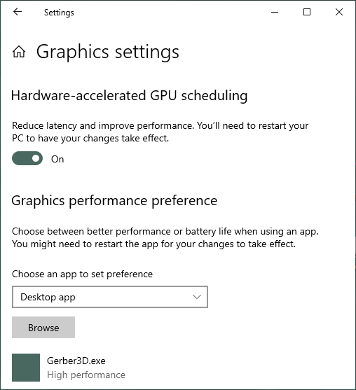
Note (1) the executable name for the ZofzPCB is "Gerber3D.exe"
Note (2) that a single monitor is connected to a single GPU in a stationary PC by using a specific display connector. The GPU switching on the fly is usually not implemented.
Also: superuser.com: why does my laptop have two graphics cards -
Disable GPU effects in Windows. Windows GDI will not wait for the GPU to be free. Windows will use the CPU instead.
windowscentral.com : how to disable system visual effects boost performance Windows 10 - Reduce ZofzPCB load on the GPU - see the topic below
How to reduce the load of the GPU?
- Remove displaying of the sides (thickness) of the layers: Menu - View / Thick Layers
- Reduce sub-sampling: Menu - View / SubSampling
- Make display window smaller
- Reduce complexity of the generated mesh. Menu - View / Render Effects
(Note that default settings are not particularly high. Use this method if you have been increasing the mesh complexity before.)
Why am I not allowed to overwrite component selection, even if the models are there?
Unlike in other 3D software, the models are created out of footprints. There must be a particular configuration of pads/holes for the generator to fit the model. Pads and footprints must always match. You never had to adjust the 3D model rotation and position or the distance of the el-cap pin, right?
Examples:- SMD shunt resistor
A resistor may look the same, but there are 4 pads on the PCB. There are 2 pads for each terminal, avoiding a voltage drop on the high current solder junction. The algorithm searches to fit a 4 pad device in this place. There would have to be some arrangement to tell the program to ignore the specific 2 pads. - Metal Can OSC
The footprint is constructed to accommodate 2 types of the package: long (like DIP14) and short (like DIP8). This dual function is not visible in the IPC-356 file. The algorithm constructs a strange 6-pin device. - 3-pin SMD diode
Diode uses only 2 pins; the not-connected pin is not exported in the IPC-356 file. The algorithm fits a 2-pin diode instead. This usually can be corrected by the settings - something like "export all".
A solution for this would be a kind of IPC-356 graphical editor, allowing for removing pads/holes or adding from the drills or copper/solder-mask pads.
Some decisions are permanent in the component selection tree (e.g. this is a 2 pin device),
and some are guesses (e.g. this is a resistor).
It is possible to overwrite any guess.
How to load the license key?
Program without the component generator license will nag you, but it will not limit any 3D Gerber functionality except the components view, View-Only saving possibility and STEP file export. You can switch off the nagging if you select Components / Model Generator / Extruded (Free)

The license changes the "Extruded" components view....

... to the "Parametric" component view.

When you have the license key, please start the "License Key" dialog box, via menu: Components / Enter License Key.

Please paste the complete license key text into the edit box, by clicking inside the box (cursor should blink there) and pressing the Ctrl-V keys on the keyboard.

The text of the License Key should appear in the edit window. The text is blurred on the picture, to keep it secret. But in the real life it is just a normal text, ending with an equal sign. Note that you should preserve the upper and lower case.

After pasting the key text (1), please check the validity of the key by pressing the [Load License Key] button (2). The info text (3) should reflect your key type and date of validity.
Now, you can close the dialog, pressing the (X) in the corner (4).

- Note that the key text is written to the registry on the program exit. If, by chance, the program is closed incorrectly, the key might not have been saved, and you may need to repeat the copy-paste procedure.