If you're a PCB electronics designer, you know how important it is to review your designs thoroughly before sending them to manufacturing.
It's costly – and embarrassing – to find design errors in a production board.
You also know how difficult it is to really check everything in CAD. You're dealing with multiple layers, so you can't see everything at once.
Plus, your CAD program generates some structures automatically – you don't see them while you're in CAD. So it's hard to visualize your finished board.
Of course, with experience and as you gain confidence in your CAD package, un-caught errors become less likely. But still…
Wouldn't it be great if you could:
- Look at your PCB design through a different set of eyes?
- Get a completely different perspective than you get from CAD or a 2D Gerber viewer?
- See your board just as it will look when it comes back from production?
- Inspect it from any angle… just like holding the finished board in your hand?
- Be able to “look between the layers” for hidden errors?
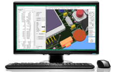
Well, now you can… with ZofzPCB.
Screenshots (new UI):
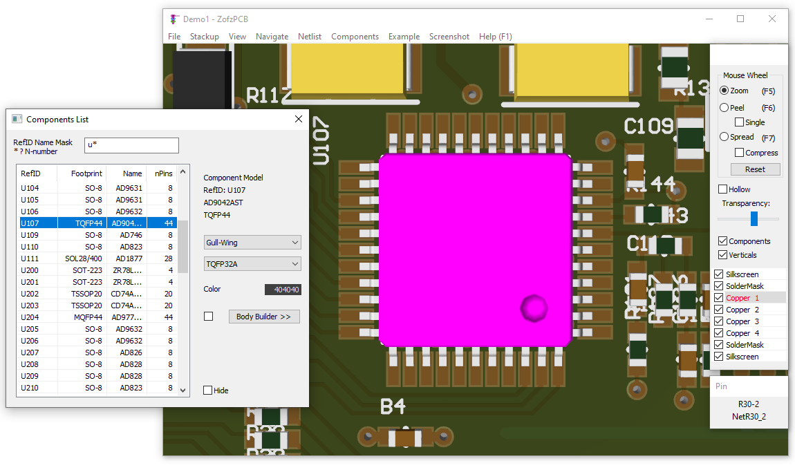
| Components List |
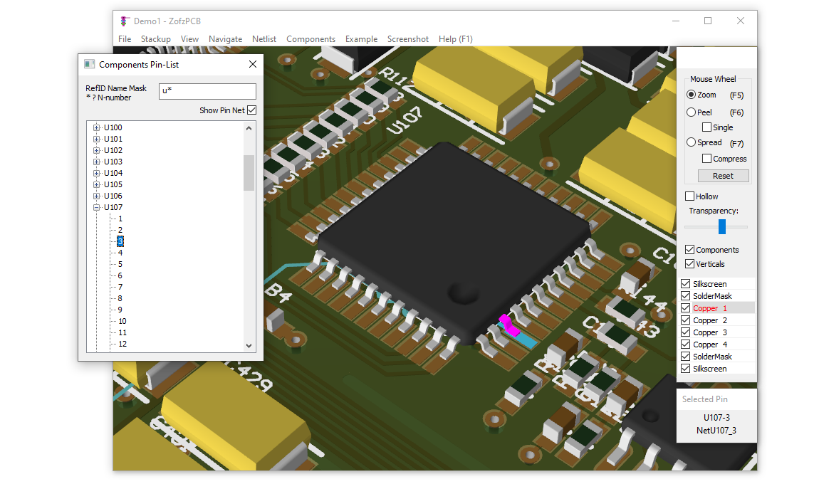
Pin List |
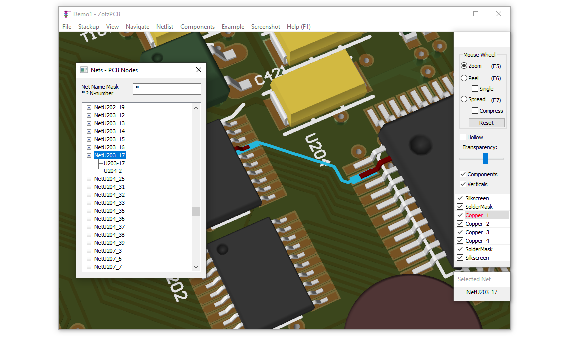
Net List |
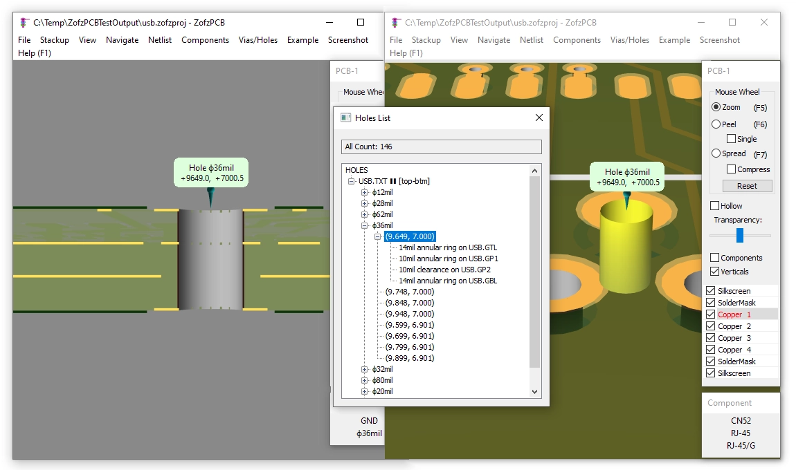
Hole List |
|
|
|
|
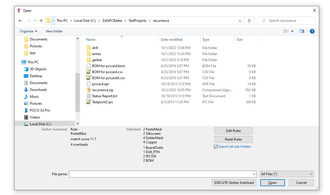
| Gerber - Autoload | Gerber -
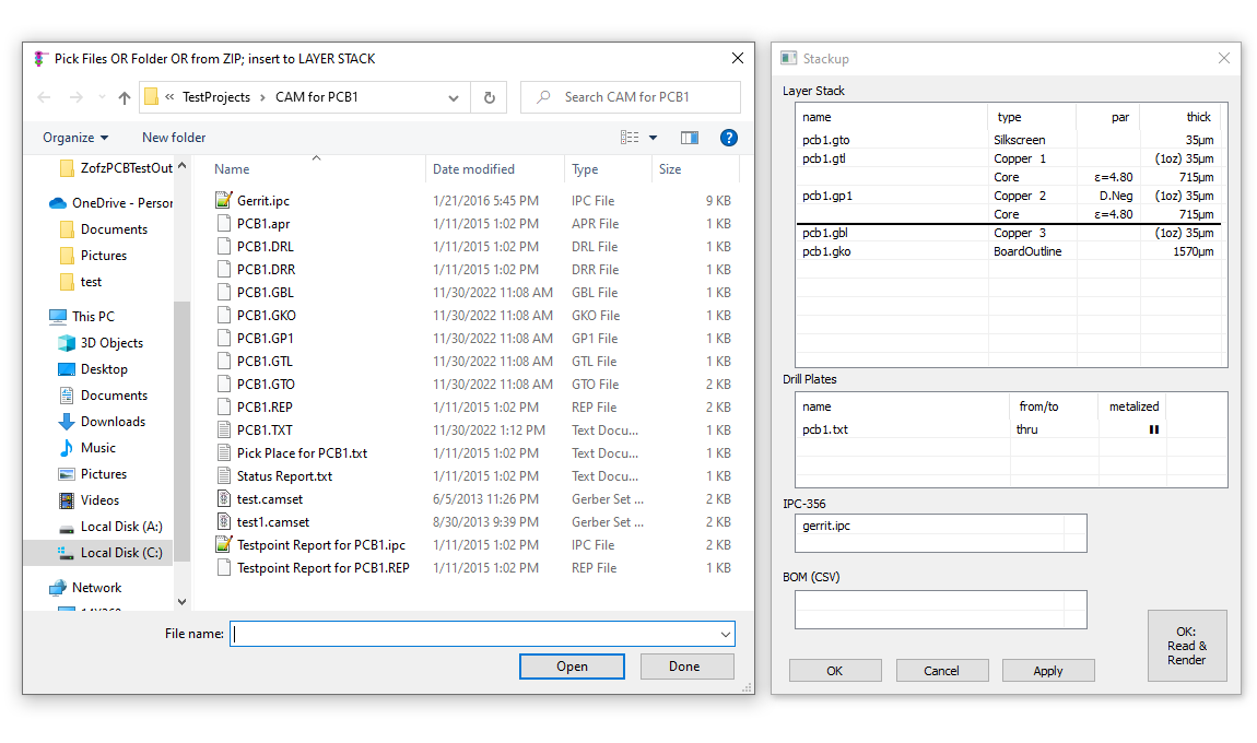
Manual Stackup Compose | Measurements | Component Models + BodyBuilder |
|
|
|
|
A Gerber Viewer that Gets “Between the Layers”
ZofzPCB is a FREE 3D Gerber viewer that shows you more than just how your board is going to look. ZofzPCB lets you see inside your board – between the layers – so you can give it a truly thorough inspection. It makes pre-production verification of your PCB designs fast, easy, intuitive and fun.
With ZofzPCB you get:
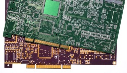
- Realistic 3D rendering from your Gerber/ODB++/IPC-2581 files that shows you how your finished board will look and unveils errors that are difficult to detect in a 2D view.
- Automatic recognition and import of Gerber, drill, netlist (IPC356 testpoints), and BOM files, saving time and reducing errors.
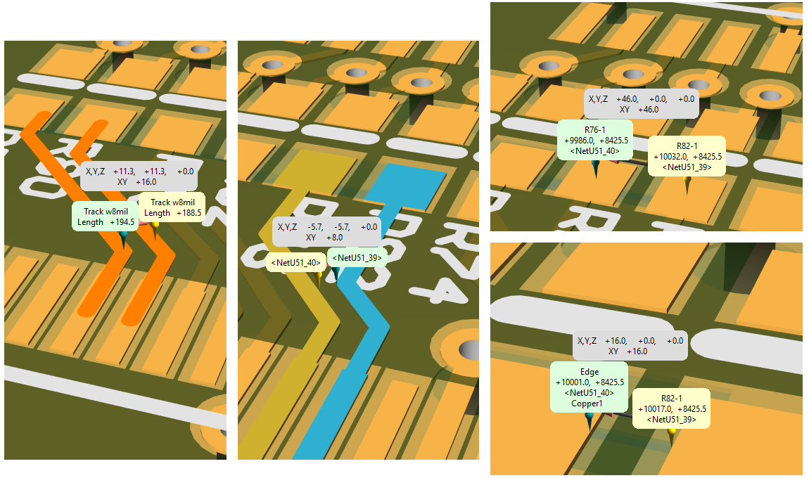
- A measurement function that shows you the X,Y,Z and XY distances between any two objects (pad, hole, track, edge, net).
- A hole browser that shows you clearances, annular ring, and cut-thru stack view.
- A vertical cut-thru view in any place at any angle.
- A Visual Comparison comparing two PCBs with color-coded differences, exposing design revisions differences.
- An export of the 3D board shape and layers to a STEP file, to be read into any mechanical CAD or a simulator engine.
- Full 3D navigation via intuitive mouse and keyboard controls lets you quickly and easily view any point on the board from any angle you choose.
- Orthogonal camera mode, allowing for a homogeneous scale, 1:1 printout and 2D mode navigation, just like in a standard Gerber Viewer.
- Color scheme selection that lets you assign colors to structures in different ways.
- Layer ON/OFF and PEEL functions let you remove any design layers in your way.
- Material density, hollowing, and layer spread controls that let you “look between the layers” and verify connections between them.
If a netlist has been imported, via IPC-356 file (Gerber) or as a part of ODB++ or IPC-2581:
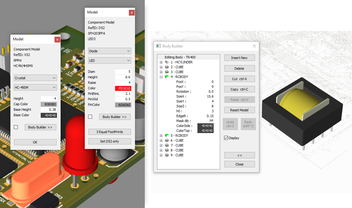
- An automatic 3D Component Modeling, instantly generating detailed 3D models from PCB footprints for seamless visualization.
- Browsing by component, pin, and netlist that lets you instantly inspect any design element.
- Automatic error checking of your image-generated netlist against the source netlist from the input file.
- STEP file contains all mounted components as a structured assembly…
and much more!
See the ZofzPCB 3D Gerber Viewer in Action
To get a better idea of how all these features work and how powerful they really are, we urge you to take a look at this brief DEMONSTRATION VIDEO:
We think this video shows just how valuable ZofzPCB can be to you as a PCB designer.
Gain New Perspective on Your PCB Designs Today!
ZofzPCB viewer makes pre-production inspection of your PCD designs fast, easy, intuitive and fun. Get started today!