3D CAD/CAM Viewer User Manual
Version: 2.0.1.0,
download as PDF
Table Of Contents
- Reading in CAD/CAM Files
- Gerber Set
- Auto Load (Gerber Set)
- Manual Compose (Gerber Set)
- Zip Files
- File format
- Board Outline, using a meta drawings
- Board Outline, identifying the PCB outline
- Automatic fit of image, drills and netlist
- Stackup file save/load
- Rendered board file save/load
- Netlist and IPC-356 file
- Components and IPC-356 file
- IPC-2581 file
- ODB++
- Gerber Set
- Components Modeler
- Body Builder
- STEP File Export
- Navigation
- Right Panel: Layers & effects
- Measurements
- Right-Mouse-Button click menu
- Cross Section
- View Menu - still some more effects
- Screenshot
- Autopilot
- Connection between Program and Website
- Bug Reports
- Program Structure Chart
- CrossCheck page
- Keyboard and Mouse Controls on a single page (PDF)
External Resources
- Gerber format specification & related documents:Ucamco Download Page
- Gerber file format at Wikipedia: Gerber Format
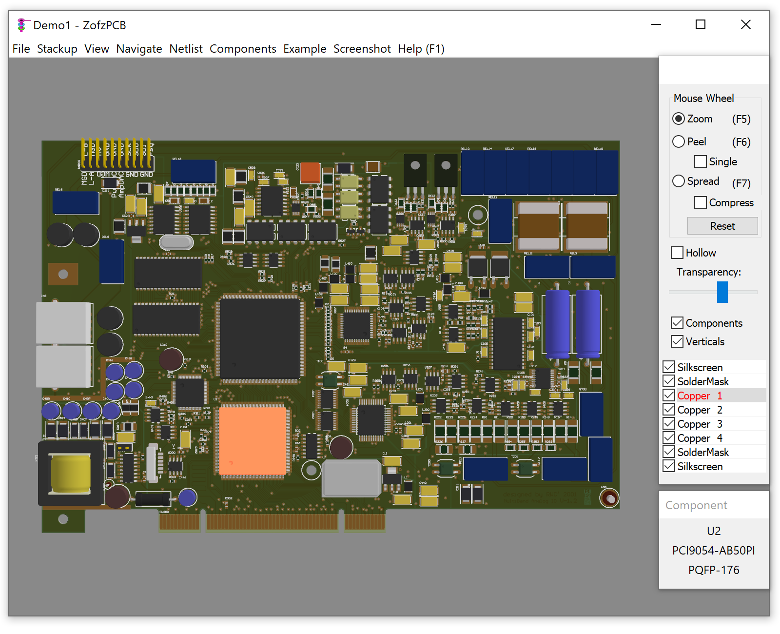
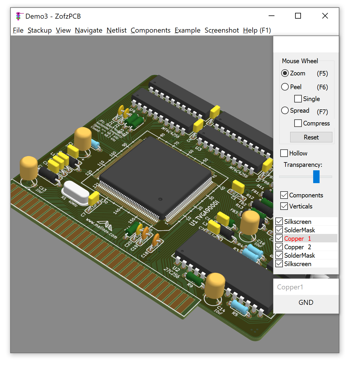
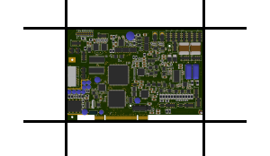
Program Screenshot - basic view, automatically loaded Demo1
1. Reading in CAD/CAM Files
- ZofzPCB can read all major CAD/CAM files formats:
- Gerber Files Set, that is: layer image files (Gerber), drill files (Excelon or Gerber), "Netlist" file (IPC-356), BOM file (CSV format).
- IPC-2581 - single file XML format.
- ODB++ - single file packed format. (planned for December 2022)
- ZofzPCB can save and load its binary file format, containing all setup and rendered board. (file-extension .zofzproj)
- Gerber Set composition, the used files functions, and all setup data and components model adjustments can be saved in a configuration file. (file-extension .camset)
Loading the .camset file (instead of the .zofzproj file) is helpful when you regenerate the Gerber files and want to reread them again.
Loading ODB++ or IPC-2581 files is straightforward. Composing back the Gerber file set needs a bit more effort. The composition can be done automatically, semi-automatically, or manually.
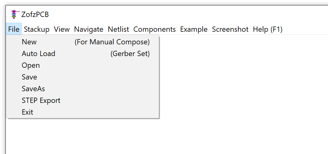
- New (For Manual Compose)
Starts an empty project, set up file explorer window and a stack dialog window.
At this point you may drag and drop Gerber-Set files into the stackup. - Auto Load (Gerber Set)
Starts up file explorer window. The discovered Gerber (and Gerber related) files are summed up in the file explorer additional display area.
You may proceed with automatic load, by pressing Execute Auto Load button. - Open
Starts up file explorer window. You can select a single file to load.
Options are: .camset, .zofzproj, IPC-2581, ODB++.
1.1 Loading In Gerber Set
1.1.1 Auto Load (Gerber Set)
Auto Load provides a quick and convenient way of composing a new project. The purpose of the Auto Load is to match Gerber/drill/IPC-356/BOM files to assumed functions in PCB definition. This feature is based on a file name rules set, located in a 'script' text file: %APPDATA%\ZofzPCB\CAM_Load_Rules.txt
The file contains a set of rules, divided into "sections" corresponding to a particular file naming schemes, like:
section KICAD (Protel Mode)
There is a list of possible file functions and related file name pattern masks in each section:
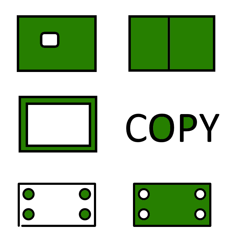
BOM                *.csv
IPC-356            *.ipc
Silkscreen T       *.gto
Silkscreen B       *.gbo
Copper     T       *.gtl
Copper     M       *.gN
Copper     B       *.gbl
Copper     M /     *.gpN
BoardOutline       *.gbr
Drill_NPTH         *np*.drl
Drill_PTH          *.drl
The pattern masks test each file; the first hit is assigning a function and finishing the search for the file.
All sections are tested, and the section with the most hits is chosen to continue the load. Finally, the hit results are displayed for acceptance.
Please refer to the CAM_Load_Rules.txt file itself for syntax explanation.
If you would like to create another set related to a particular CAD vendor default convention, then I am willing to assist you. Get in touch with me.
To access the rules text-file, use the button on the Auto Load dialog.
Alternatively, you can use the following file path: %APPDATA%\ZofzPCB\CAM_Load_Rules.txt
Steps:
- After launching the program, go to the menu "File". Select Auto Load. That is Menu: File / Auto Load.
- The following dialog box will appear:
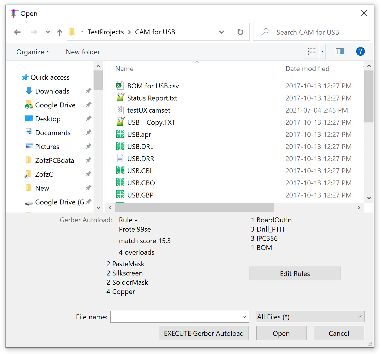
- Select Folder.
A summary of matching files is displayed extension area of File Explorer. Sometimes you may find that the matching of files significantly differs from expected. In such cases, you are advised to use the manual method. - Press EXECUTE Gerber Autoload.
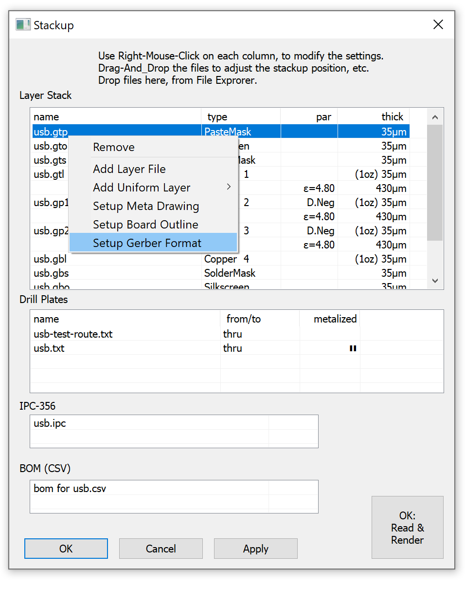
- The layer Stackup dialog box is displayed. (See screenshot below.) The dialog allows you to review Gerber files assignment to particular layers, drill, IPC-356 netlist, and BOM slots.
- If you want to add or remove some files, please right-click in the file name column and select "Remove" or "Add Layer File". Please refer to the section "Manual Compose" below.
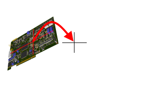
- Press OK: - Read & Render. This command will flatten the board. The program will convert the negative and positive constructs into simple flat shapes. The board polygons are then triangulated to enable the Direct3D to display the PCB model.
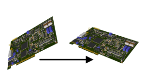
1.1.2 Manual Compose (Gerber Set)
Have you tried the auto compose and you are not satisfied with the results? If that is the case, then you can compose your project by using manual compose. The procedure of composing a project using this approach is as detailed below.
Steps:
- After launching the program, go to menu "File". Select New (For Manual Compose). That is, Menu: File / New (For Manual Compose)
This command will create a clean new project. - Assign files to read
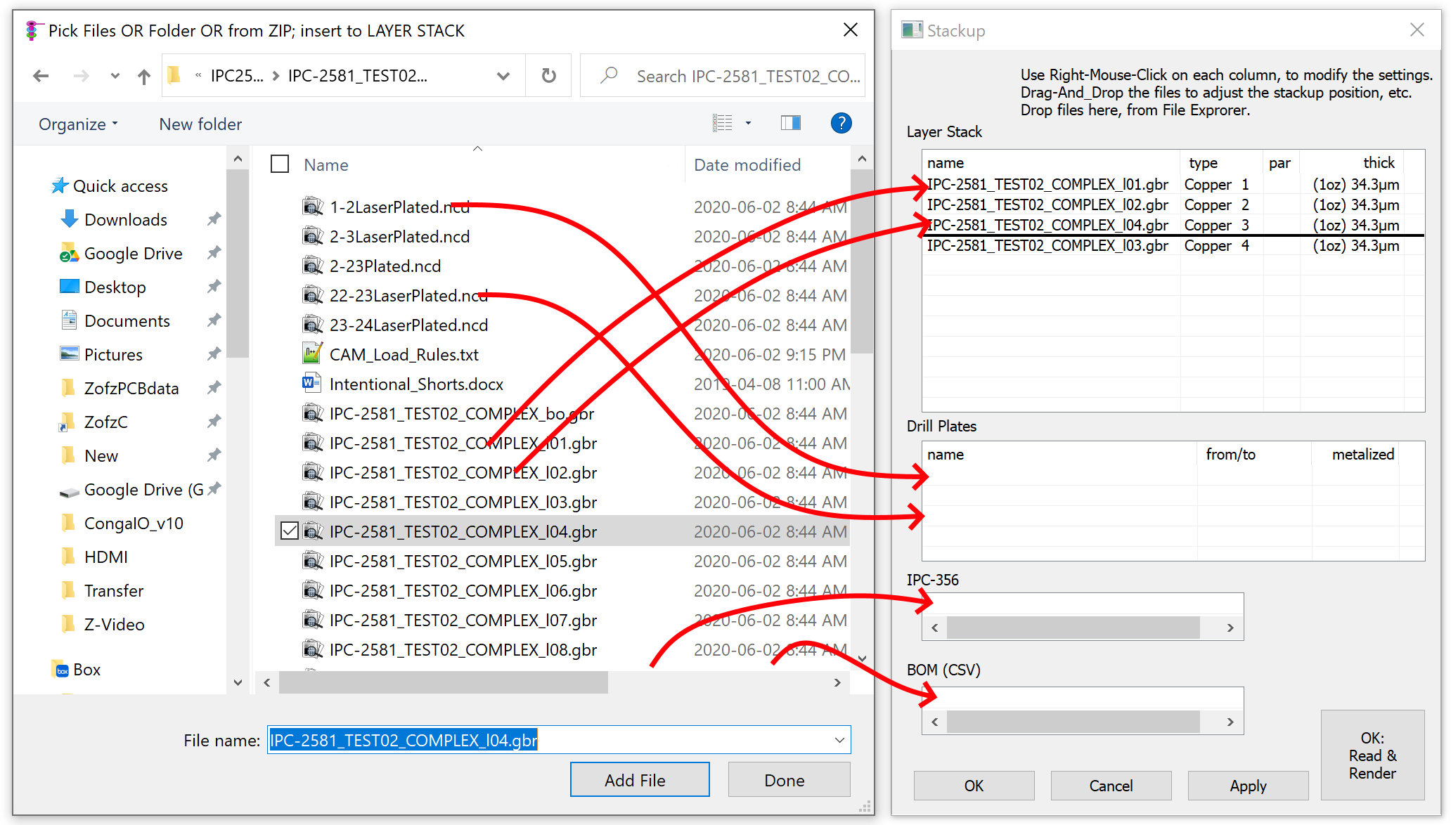
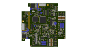
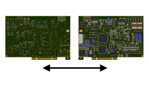
- A Stackup dialog box, like on the right side of the picture above, will appear. Additionally, the program creates a File Explorer dialog,
like on the left side of the image above. The Stackup dialog box contains: (from top)
- Layer List (including the board outline, as the last item),
- Drill Plates List,
- IPC-356 Netlist file place-holder
- BOM file place-holder
- Configure required Gerber-Set files by drag-and-dropping them from Explorer to the Stackup dialog.
- Alternatively, you can use the Add File button on the File Explorer, first selecting the destination in the Stackup dialog.
- You can drag and drop files inside the Stackup dialog, e.g., from Layer List to Drill Plates.
- You can drag-and-drop multi-file selections.
- You can use Windows File Explorer you have evoked yourself.
- Adding core/prepreg to the stack can be done by right-clicking the "name" column and selecting the "Add Uniform Layer" menu.
- You can close the File Explorer when all files are in the Stackup dialog.
- A Stackup dialog box, like on the right side of the picture above, will appear. Additionally, the program creates a File Explorer dialog,
like on the left side of the image above. The Stackup dialog box contains: (from top)
- Organizing Layer Stack
- If needed to recall the Stackup dialog, use Menu: Stackup / "Display/Edit"
- The stack list represents the order of layers from top (component side) to bottom (solder side).
Each entry represents a layer in the PCB layer stack. It is important to note that some layers are associated with Gerber files (e.g., copper),
while others are not (e.g., core).
You can edit the layers' order moving a selected layer (or group of layers) up or down by using drag-and-drop. - The columns:
name shows filename if the layer is associated with a Gerber file type the type of the layer, like solder-mask or copper, etc. par additional parameters thick the thickness of the layer. For copper, you can use 'oz' - oz per square foot (for Europeans: robots have square feet) - The Board Outline field is a special layer and should be positioned at the bottom of the list. It may or may not be related to a Gerber file. It is a placeholder for the PCB total thickness value.
- When all the Gerber layers are identified, it is easy to enter the total thickness of the PCB in the Board Outline's Thickness field. The program will adjust the thickness of the core/prepreg layers only.
- The Gerber file should internally specify whether the "film" is positive or negative.
For some old Gerbers, this information may be missing or given wrong. To understand the positive and negative films, consider this scenario: if you want to draw a punched surface, you can draw the dots and ask for a negative film. Alternatively, you can paint the entire surface except for the dots and ask for a positive film.
The options are:default positive [ ] - If there is no information in the Gerber header, set to positive default negative D.Neg - If there is no information in the Gerber header, set to negative force positive F.Pos - Ignore information in the Gerber header; always set to positive force negative F.Pos - Ignore information in the Gerber header; always set to negative - A rule is to draw the paste and solder masks in a negative option. If the Gerber is drawn in opposite polarity, you can use the above setting to force a specific polarity.
- Organizing Drill Plates
See the image above (again)- The columns:
name - shows filename (Excellon or Gerber) from/to - vertical start and end copper numbers metalized - type of the hole, see below - The software detects whether the provided drill file is in Excellon or Gerber format.
- Sometimes, a PCB project will have only one drill file (default is plated and through). If that is not the case, you will need to define the functions of the provided drill file(s).
- Define where the drill plates start and end - for example, assuming a 4-layer PCB, from copper layer 1 to copper layer 4 (top to bottom) or copper layer 1 to copper layer 2.
- The program also allows you to specify one of the following options:
Non-Plated - plain, nonconductive hole Plated - conductive barrel Filed - conductive barrel, metal filed, or capped µVia↓ - conductive barrel and bottom - metalized from outside µVia↓ Filed - conductive barrel top and bottom - metalized from outside µVia↑ - conductive barrel and top - metalized from outside µVia↑ Filed - conductive barrel top and bottom - metalized from outside - Drill files may contain holes and routing. If you have routing on a separate file, add both files to the Drill Plates.
- The columns:
- OK: - Read & Render
- The program will flatten the board. It will convert the negative (cutouts) and positive constructs to simple additive shapes. It is then triangulated for the Direct3D to display the PCB model. This step is crucial for high frame rate animation.
- In case there is a need to interrupt the process, the following options are available:
- Stop At the Next Checkpoint
The process will be stopped when the current task ends. No new actions will be started. - Stop Now Dangerously
The process is stopped immediately. This action causes the allocated memory to leak. It is not guaranteed that the process will continue from the point it is stopped without restarting the program.
- Stop At the Next Checkpoint
1.1.3 Zip Files
The file explorer and auto detection feature, described above in this chapter, emulates zip files as directories. Reading in all the CAM files and .camset files and saving the .camset file works the same way.
IPC-2581 files can be also extracted from the zip folders.
This feature does not apply to the binary zofzproj files, which have LZMA compression on its own and cannot be read or written into a zip file, by ZofzPCB.
This feature does not apply to the ODB++ files, which may have gz compression on its own and cannot be read or written into a zip file, by ZofzPCB.
The above functionality works only with zip files, but not with 7z or rar files.
1.1.4 File format
You should not change the following options unless the Gerber files are generated by an old or incompatible CAD exporter or are abnormal in any other way.
- Gerber file options
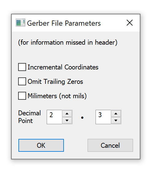
Access: Right-Click on "name" column of the Layer List, Stackup dialog.
The contemporary format, RS-274-X or GerberX2, defines apertures and all parameters needed to create a layer drawing. Sometimes, only a subset of parameters is defined by the Gerber file. The operator has to define missing settings manually. Nevertheless, such cases are rare. Parameters set in the associated dialog are default. If there are explicit definitions in the Gerber file, they normally override the defaults. A default negative parameter is defined per layer in the layer stack list. - Apertures
The long-depreciated pure D format cannot be used, as, at least, the apertures must be defined in the file.
If that is not the case, you should manually add file headers containing apertures definitions. It is important to note that the apertures should be in RS-274-X file format. - Excellon file options
Access: Right-Click on "name" column of the Drill Plate list, Stackup dialog.
Although we have few parameters here, the standard is generally weak. I hope the "Guess" option will work for you. If it doesn’t, kindly feel free to send me your examples.
The Guess option is based on a statistical approach. Guessing is done by matching and scaling drills to pads. Gerber format offers a better quality output than Excellon, making it the preferred format for drill files.
In some cases, especially when a small number of holes is placed on a PCB or holes are not related to pads, the Auto-Offset may destroy perfectly aligned file. You can switch off the Auto-Offset procedure by unchecking the check-box. The offset between Gerbers and drills is then assumed to be (0,0) - IPC-356 file options
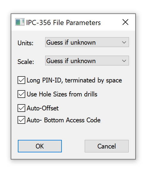
Access: Right-Click on "name" column of the IPC-356 filename box, Stackup dialog.
This constant column format defines a specific number of digits per value and this may differ with what some projects may require. For that reason, some vendors prefer to change the scale while maintaining the required number of characters in order for the format to handle bigger boards. Another problem might be missing units definition or unspecified pads sizes. Additionally, limited space for the component designator and pin names makes it hard to decide what to do, when a longer text is used in ECAD. Either the names will be truncated/renamed or the column positions are destroyed. In most of the cases, it is possible to recover. The recovery mechanism may fail, however. Therefore it is possible to disable the specific automatic corrections.
Note that truncating the names may result in "short-circuits" or miss matching with the BOM, disabling some of the ZofzPCB features.
1.1.5 Board Outline: using the meta drawing
This approach can be used when the board outline is drawn on a copper or silkscreen layer.
However, the approach is suitable only if the outline is drawn using tracks of thickness below a specific threshold value.
All other objects on the layer must use a thickness value that is greater than the threshold. The threshold thickness value is set in the dialog box as shown below.
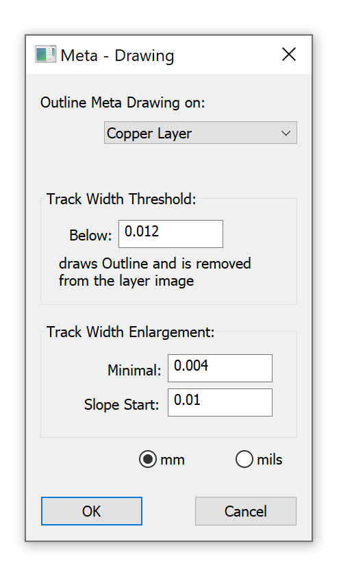
Access: Right-Click on "name" column of the Layer List, Stackup dialog.
 Additionally, this dialog box enables the program to deal with the finite accuracy of the geometrical calculations.
This helps to avoid the disappearance of tiny objects or the problems that could result from their inclusion.
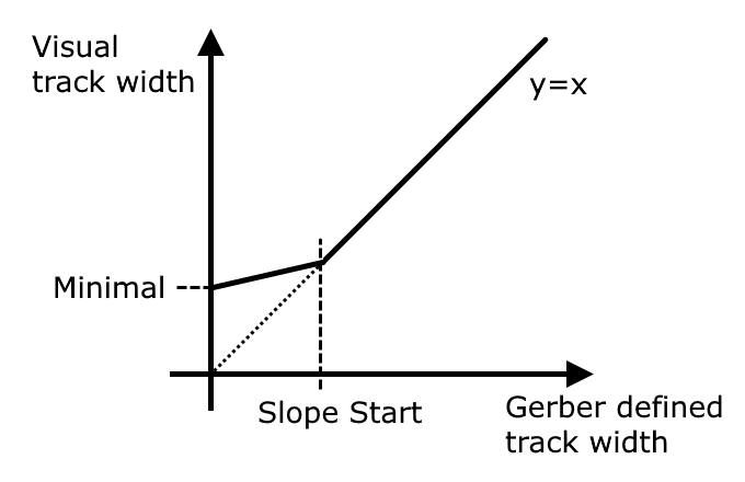
The program offers a correction function that is applicable for objects that are below a specified size.
Additionally, this dialog box enables the program to deal with the finite accuracy of the geometrical calculations.
This helps to avoid the disappearance of tiny objects or the problems that could result from their inclusion.
The program offers a correction function that is applicable for objects that are below a specified size.To ensure uniformity of a correction, 2 values are used to define the new slope of the transfer function. By keeping the value of "Minimal" less than that of "Slope Start", the size relation between the affected object sizes is preserved.
1.1.6 Board Outline: identifying the PCB outline
Sometimes the Gerber files are generated as pure M2M files. In other cases, a descriptive text or drawings is inserted in various layers.
The program can remove any object that is located outside the PCB on any layer. In order to do this, the program must understand the PCB shape.
To achieve this, it analyzes the Board Outline layer (or meta drawing on other layer) to determine the M2M part of the picture
and removes objects that are outside the bounding rectangle.
You can enlarge the created mask by adjusting the horizontal and vertical margin values.
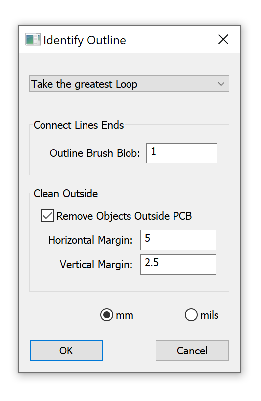
Access: Right-Click on "name" column of the Layer List, Stackup dialog.
The program offers the following options:
- Accept all detected Loops
All detected outlines define multiple PCBs. - Auto Recognition
This is based on finding a division line. The horizontal or vertical line divides the drawing into two parts: the PCB and the description text. - Take the greatest Loop
This assumes that the biggest object is the PCB. - Take 2,...10 greatest Loops
Assumes that the biggest two to ten objects are the PCB parts. You should select the number of loops that you want the program to take (from 2 to 10).
In all the above cases, the outline is converted into a polygon that represents the surface of the PCB.
On the outline drawing, the program interprets the tracks as the edges of the polygon. This means that the drawing must form a loop.
To account for small errors, the program uses the drawing track width plus "Brush Blob" value as an error margin.
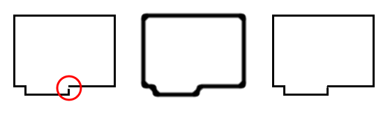
These are illustration examples of how Outline Drawings are converted to board surfaces.
The green part represents the PCB while the black one (removed part) is the drawing.
- The surfaces XOR if the borders do not touch. You can create cutouts.
- If multi-path outline is detected, the greatest surface is assumed.
- Double line means two edges (XOR). If you want to draw a frame, you should open it.
- If text is sneaking in, it will look like strange very small PCB pieces
- Small breaks may be corrected, but bigger ones may simply remove the surface resulting in a no PCB volume at all.
1.1.7 Automatic fit of image, drills and netlist
It is common to have the Gerber file image centered on the film. The drill file features an arbitrary
offset and the same can also apply to the IPC-356 file. Owing to this, offset correction is always executed.
If the points required to match are not enough, a warning usually pop ups. This message can be ignored but
you should consider the possible causes of this before you proceed.
The image/drill correction is not performed if the drill files are in Gerber format.
1.1.8 Stackup file save/load
- You can save the project configuration, go to the menu "File", and select "Save As".
A file explorer dialog will pop up, allowing for a directory selection. "Save As Type" dropdown - select ".camset" file type. Add the file name and press Save As button. - When configurations change and you wish to update your saved data, use Menu: File / Save.
- If you wish to restore the configuration, load the old project,
Use Menu: File / Load, select the .camset file. - The project configuration file type is associated with the program. That means it is possible to double-click on the .camset file to have it opened, assuming the Gerber files are still there.
The configuration file uses XML text format - you can use it in automated workflow or erase sections by hand, using a text editor if you need to.
List of configuration settings saved in the .camset file:
- Stackup, including file names, layer parameters, etc...
- Drill Plates, including file names, from-to, type
- IPC-356 file name
- BOM file name
- Color settings
- Additional layer types
- Gerber File Parameters
- Drill File Parameters
- IPC-356 File Parameters
- Board Outline Meta Drawing
- Identify Outline Settings
- Camera Positions Table
- NetList Colors
- List of Component Models parameters and Body Builder models
1.1.9 Rendered board file save/load
- You can save the complete rendered project, go to the menu "File", and select "Save As".
A file explorer dialog will pop up, allowing for a directory selection. "Save As Type dropdown" - select ".zofzproj" file type. Add the file name and press Save As button. - When any project data changes and you wish to update your saved data, use Menu: File / Save.
- If you wish to load the saved project,
Use Menu: File / Load, select the .zofzproj file. - The project configuration file type is associated with the program. That means it is possible to double-click on the .zofzproj file to have it opened.
- The .zofzproj file uses a binary compressed (LZMA) encrypted file format.
- When entering the Save As file name in the premium-licensed program, it is possible
to select to save the file in the View-Only mode.
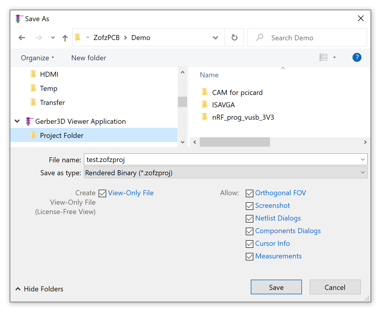
In the View-Only mode, the premium component view can be displayed using the Gerber Viewer without the premium license. That is, you can share your premium PCB view with your clients or the broad public without a need to purchase additional premium licenses.
please refer to: zofzpcb.com/ViewOnly and pcbmodel.com
1.1.10 Netlist and IPC-356 file
Please generate and include the IPC-356 Bare Board Flying Probe Test File
in your Gerber files set.
Refer to zofzpcb.com/Components
for a description of IPC-356 file format usage concepts.
The benefits of using the IPC-356 in this program include the following:
- The program tests the PCB connectivity and generates an interactive-error report if the IPC-356 does not match the copper connections.
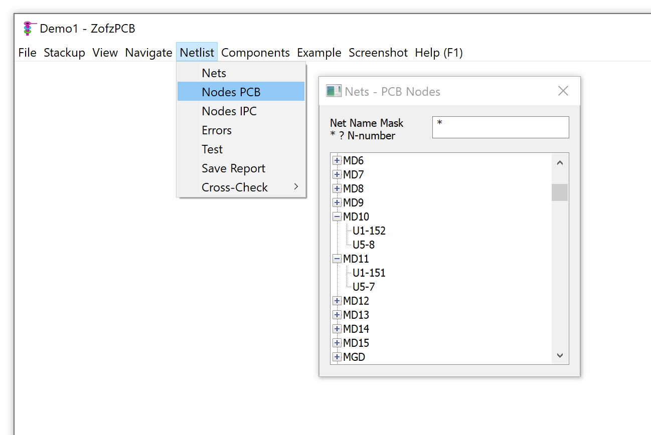
- Menu: Netlist / Nets
Display list of nets, allows for finding nets by highlighting and zooming on the selected net. - Menu: Netlist / Nodes PCB
Display a list of discovered PCB copper nets. You can expand any net to display a second-level list of endpoints (pins).
Selecting any endpoint results in highlighting and zooming on it.
"Nodes PCB" means that it is related to the copper data on the PCB when copper differs from IPC-356 - Menu: Netlist / Nodes IPC
Display list of IPC-356 nets. You can expand any net to display a second-level list of endpoints (pins).
Selecting any endpoint results in highlighting and zooming to it.
"Nodes IPC" means that it is related to the IPC-356 data, when copper differs from IPC-356 - Menu: Netlist / Errors
Display list of differences between detected copper connections and IPC345 netlist. - Menu: Netlist / Test
Re-runs the comparison test between the copper connections and the IPC345 netlist. - Menu: Netlist / Save Report
Allows to save the results of the comparison test between the copper connections and the IPC345 netlist. - Menu: Netlist / Cross Check
Cross-Check allows you to browse schematic and PCB simultaneously. ZofzPCB must be connected to a schematic editor, such as OrCad Capture. For a demo, you can visit the CrossCheck-Page.
The unrolling sub-menu allows for configuration of the keyboard keys and mouse functions used for sending cross-check commands, to the schematic editor program:Disabled - comands are not send, P & N keys act for selection CPN: Comp Pad Net - C, P, N keys are used for crosscheck; selection disabled C: cross-check - C key is used for crosscheck; P & N keys act for selection On Hover - mouse hover hits invoke crosscheck commands; P & N keys act for selection
1.1.11 Components and IPC-356 file
Please generate and include the IPC-356 Bare Board Flying Probe Test File in your Gerber files set. In addition, please refer to zofzpcb.com/Components for a description of IPC-356 file format usage concepts.
The benefits of using the IPC-356 in this program include the possibility of displaying components, just like in assembled PCB. There are two variants of the components model generators:
| Extruded | Free option Extruded option provides elementary shapes related directly to the footprint dimensions. |
| Parametric | Premium option The modeler recognizes the footprint shapes, additionally using the component designator text to select the model type. You can overwrite the guesses using other models with compatible footprints. You can adjust detailed dimensions and colors. Number of parameters depends on the model, however. |
Please note that there is no direct data about the THT component top/bottom side in the IPC-356 file. The modeler places components on the top side by default. You can swap any THT component to the other side manually.
It is crucial to save your decisions about model selection, parameters, THT side in the .camset or the .zofzproj file.
Access to functionality related to the components and IPC-356 file:
- Mouse hover Right Panel Info
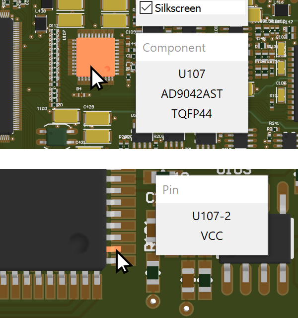 Display component designator and data from the BOM file:
- Component - RefID, Name, Footprint
- Pin - RefID-PinID, Net Name, Hole Diameter (not shown here)
- Mouse Right Button click on a component
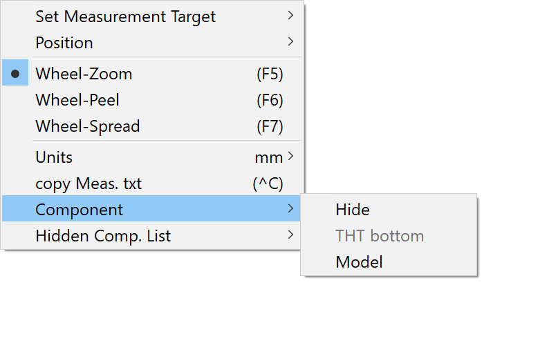 Displays the Right Click Menu, where some actions can be called in the "Component" section:
- Hide - Hide the component
- THT bottom / top - swap THT component to the other side
- Model - show Model Dialog Box
- Hidden Comp. List - Show List of components to unhide
- Menu: Components / Component List
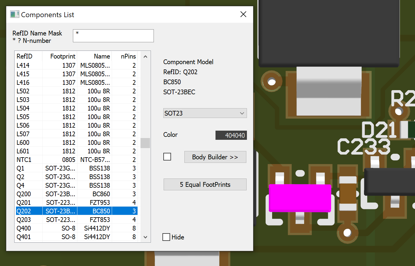
Component browser.
(Component browser uses information from the csv BOM file, if loaded.) You can preselect components using the Mask field.
Please do not use capital letters. The search is case insensitive.
'*' means any text, '?' means any character, and capital 'N' means any number.
Selecting any component from the component list zooms it into direct view. The selected part is marked pink.
After selecting the desired component, Model parameters are shown on the right side of the dialog, allowing for modification.
Please refer to the next chapter, for the Modeler description. - Menu: Components / Pin List
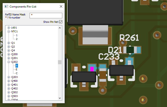
Component browser and pin browser.
You can preselect components using the Mask field.
Please do not use capital letters. The search is case insensitive.
'*' means any text, '?' means any character, and capital 'N' means any number.
Selecting any component from the list zooms it into direct view.
The selected part is marked pink. You can expand the list by clicking the plus box.
Tree-list will show the component's pins. Selecting any pin highlights it pink.
Optionally (Show Pin Net checkbox), the copper netlist connected to the pin is also highlighted. - Menu: Components / Model Generator
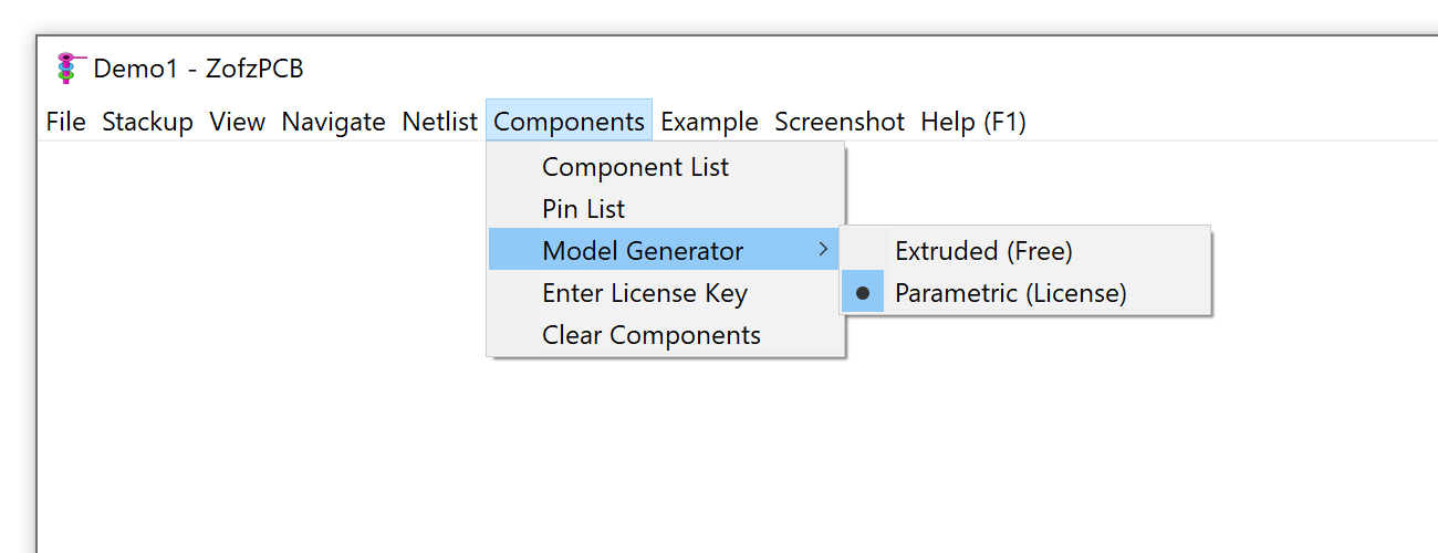
There are two options: the free and simple modeler and the premium parametric modeler, as mentioned above.
If you have enabled premium option, and have no premium license, the program nag you to buy the license. -
Menu: Components / Enter License Key
Step by step guide is located in: zofzpcb.com/FAQ - How to load the license key -
Menu: Components / Clear Components
In case when you have been reassigning the Reference ID set, in the ECAD, like running automatic annotation from scratch, stored model data is totally inadequate. There is no automatic or semi-automatic recovery function, from this situation, yet.
You may choose to just erase all stored data and run the recognition function again.
1.2 Loading In IPC-2581 file
- Menu: File / Open
Open the IPC-2581 file using the Windows File Explorer dialog. Use file name extension filter: "IPC-2581 (*.xml;*.cvg)"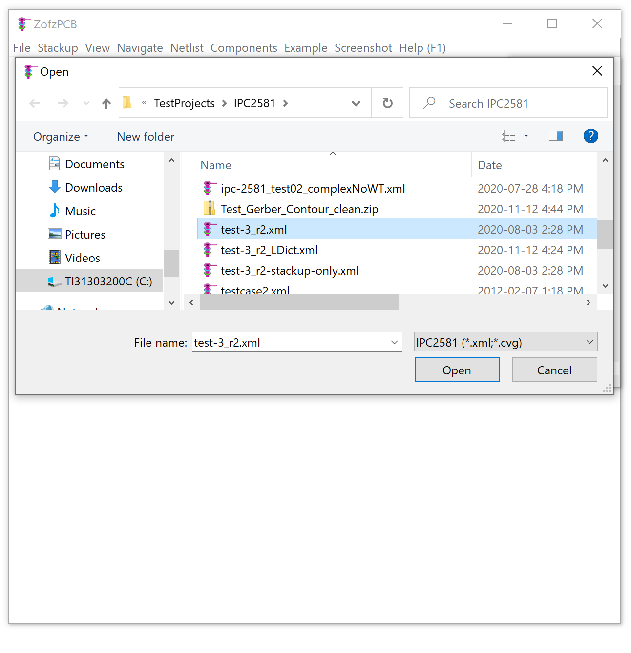
- Stackup Dialog pops up on a successful file read.
Check the layers and drills. The IPC-2581 file may not contain complete stackup information, like the position of cores or vertical dimensions.
In such a case, set the total board thickness. This operation will add missing cores of a required thickness.
Use the right-click on a proper column and row to adjust the parameters.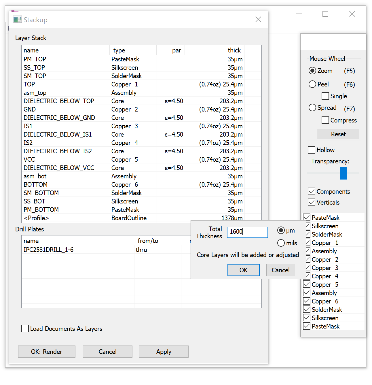
- Press: OK: Render button
The layer image will be flattened and triangulated.
The 3D PCB model will show:
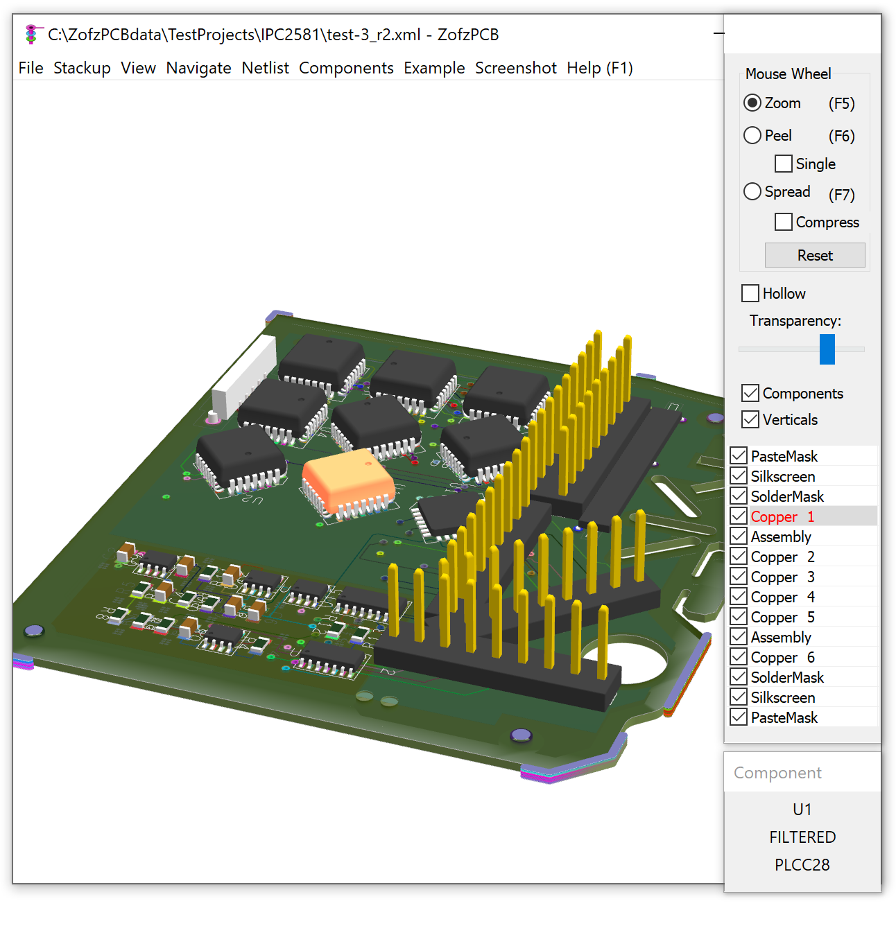
- The IPC-2581 file usually contains:
- Board profile (the equivalent of board outline drawing in the Gerber set).
The image semantics is defined, unlike the board drawing. You do not need to set up any drawing-interpretation settings.
- Netlist information (equivalent of IPC-356 file in the Gerber set).
Refer to Gerber topic Netlist and IPC-356 file - Component list (equivalent of the csv BOM file in the Gerber set).
Refer to Gerber topic Components and IPC-356 file - Sometimes, also the stackup dimensions.
- Board profile (the equivalent of board outline drawing in the Gerber set).
- You can save the rendered board, your settings (especially component model modifications) to the .zofzproj file.
- Saving to .camset file is not supported yet.
1.3 Loading In ODB++ file
This chapter is not yet present.
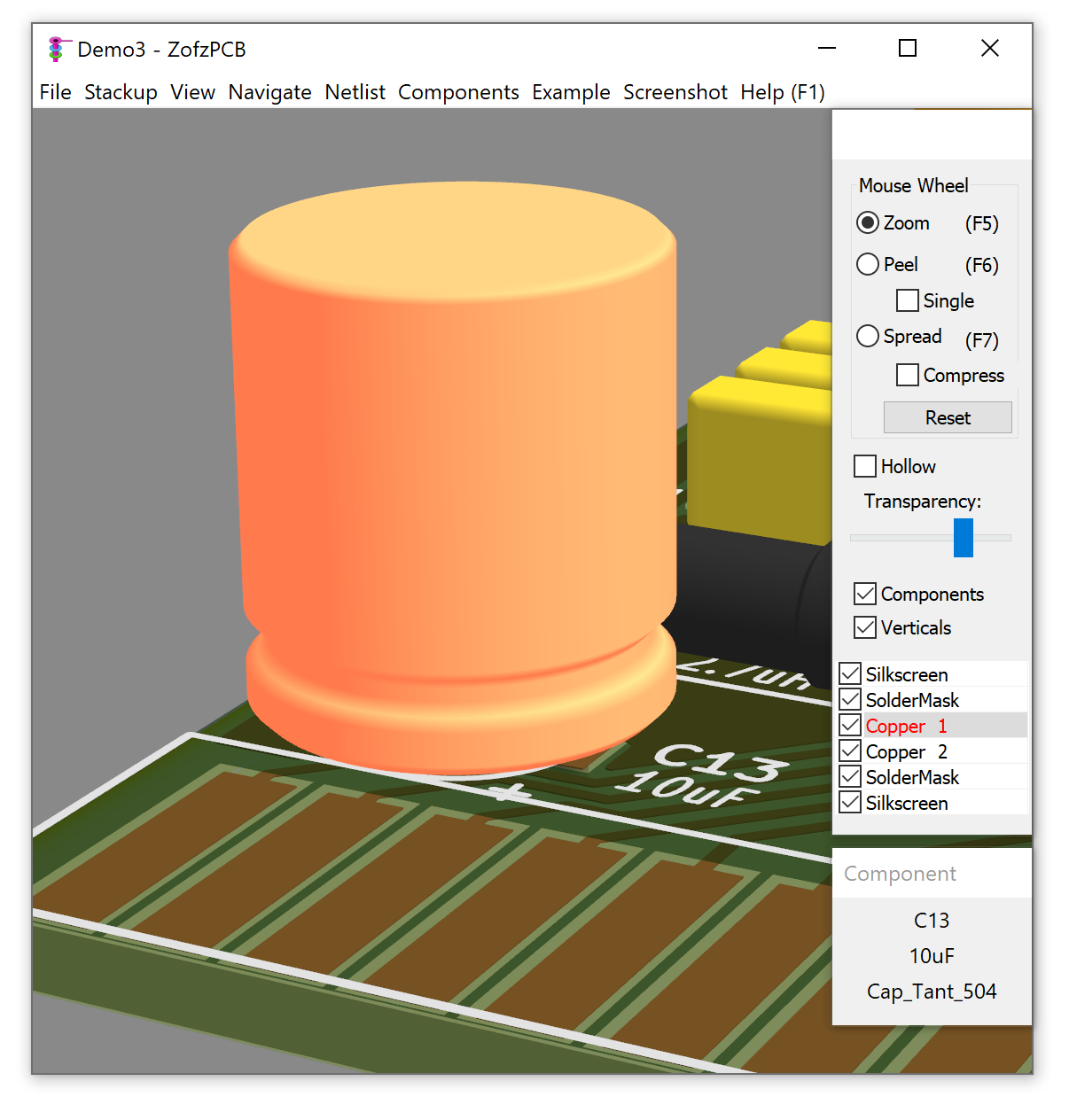
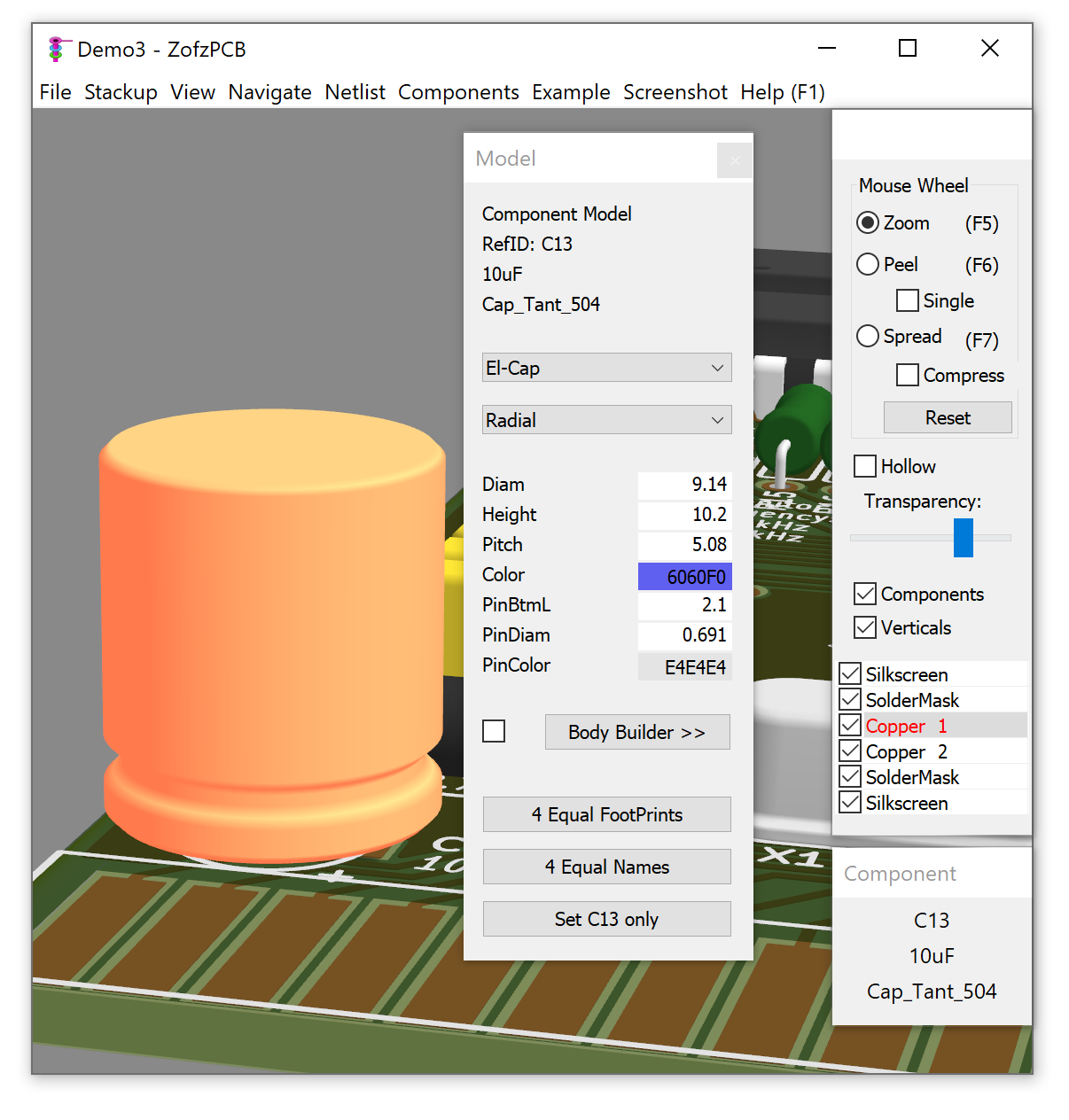
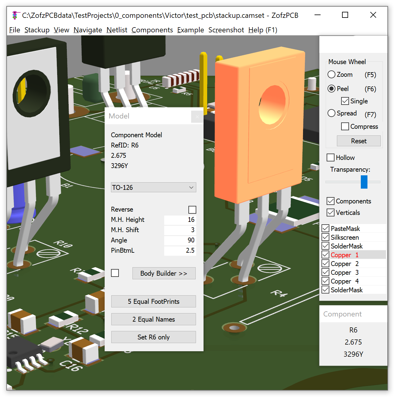
2. Components Modeler
The component model is created based on the "meta-data" of the footprint. It does not exist without the underlying footprint. For more information on this process, see the Components Page.Example: Adjusting the size of an electrolytic capacitor
-
Automatic model detection makes decisions based on the footprint geometry and designator ID.
Some decisions (detections) are "hard" - considered correct, for example, a number of pads;
some decisions are "soft" - guesses. The guesses are possible to be overwritten.
In the el-cap example, the automatically selected model was correct in that it is an electrolytic capacitor, but of course, the size is wrong:
- Access to the Component Model dialog (two ways):
- Menu / Components / Component List then, select the component using the ListView control in the dialog.
- Right Mouse Button Click on the component, selecting Components / Model on the pop-up menu.
-
Adjusting values for Diameter, Height, pin-Pitch, Pin-Diameter, and Pin-Color.
The values are taken from the part pdf; colors are taken from the picture on the distributor website, using Drag & drop pipette tool on the color dialog.
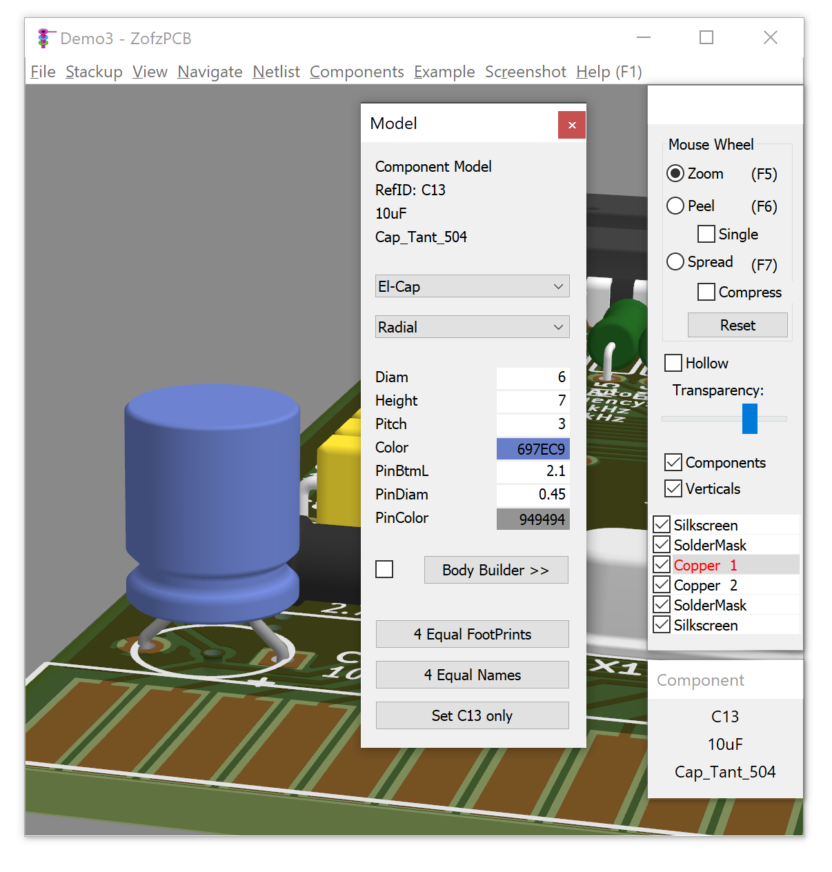
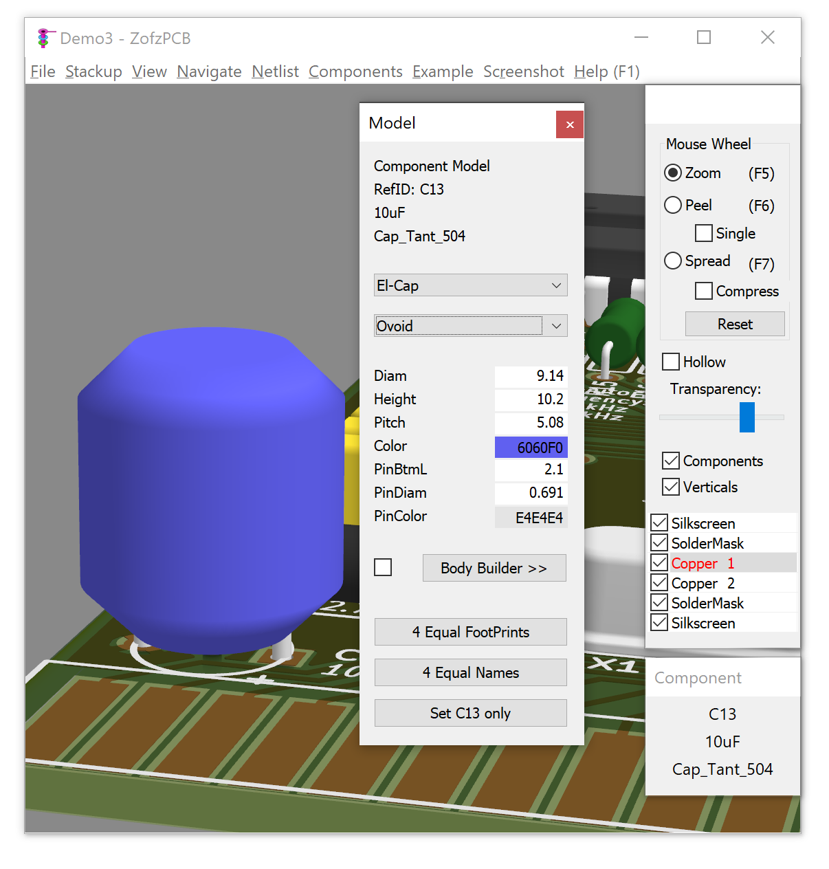
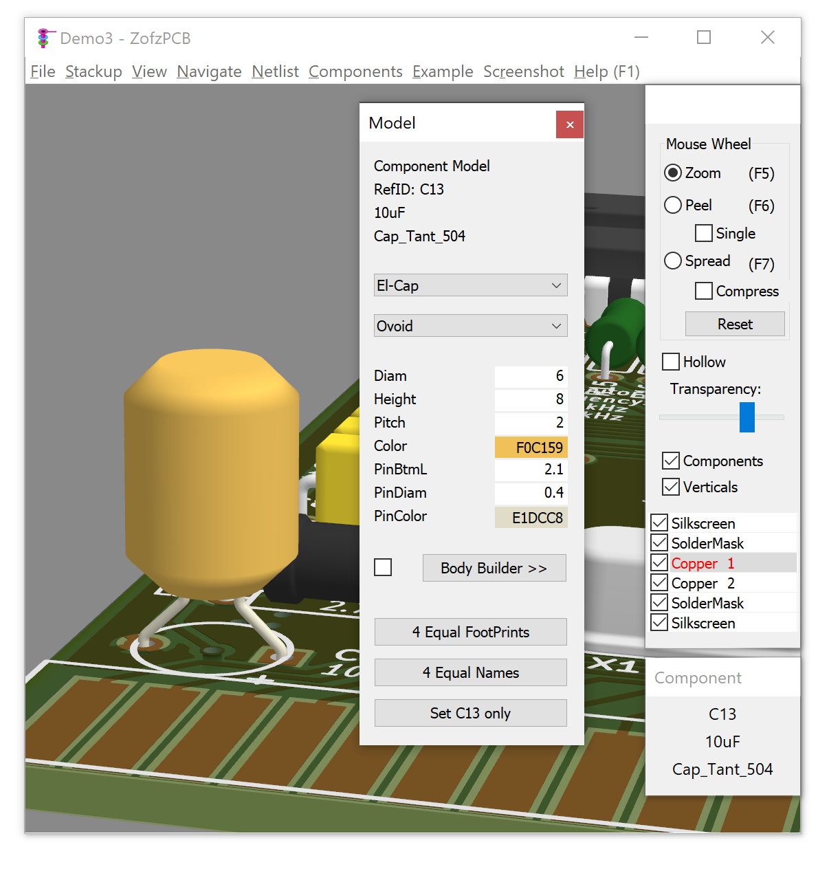
- But in this case, the wrong capacitor type was selected as a source model. It was supposed to be a tantalum capacitor!
Selecting "Ovoid" as a subcategory.
Drop-down boxes from top to bottom of the dialog represent user alterable decisions. Selecting a top category runs automatic detection on the subcategory below, including loading default values for parameters.
-
Adjusting values for Diameter, Height, pin-Pitch, Pin-Diameter, and Pin-Color.
The values are taken from the part pdf (this time the tantalum capacitor), and colors are taken from the picture on the distributor website, using Drag & drop pipette tool on the color dialog.
-
Thanks to loaded BOM, it is possible to copy the changes to the other components,
having the same footprint name or the same part name.
See the buttons on the bottom.
Please remember either to save the stackup-setup file (.camset) or the rendered file (.zofzproj).
The model parameters are saved, along with the respective data, in both file formats. (note: .camset is not yet supported on the IPC-2581 format.)

YouTube: Parametric Component Library (old UI)
3. Body Builder
Body for a Variable Resistor
- The correct element model is not in the library; the program has been deciding on another model.
This is the case where the Body Builder function will be helpful. As the Body Builder does not yet handle pins,
the best is to select another component, with the pins the most resembling what is needed, as the new model base
Way to access the Component Model dialog:- Menu / Components / Component List, select the component, using the ListView control in the dialog.
- Right Mouse Button Click on the component, selecting Components / Model on the pop-up menu.
- The 'Extruded' simplified model is a straightforward choice for this case, as it has straight round pins.
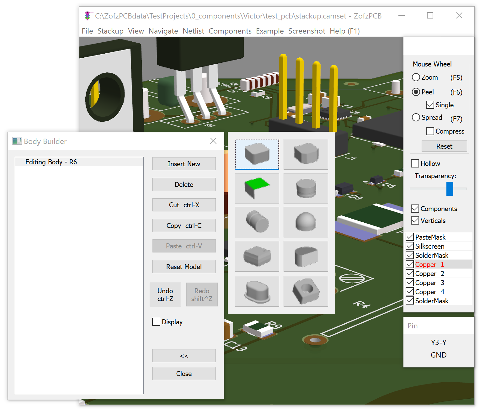
After selecting 'Extruded' in the first drop-down control, press the Body Builder >> button.
The Body Builder dialog shows up: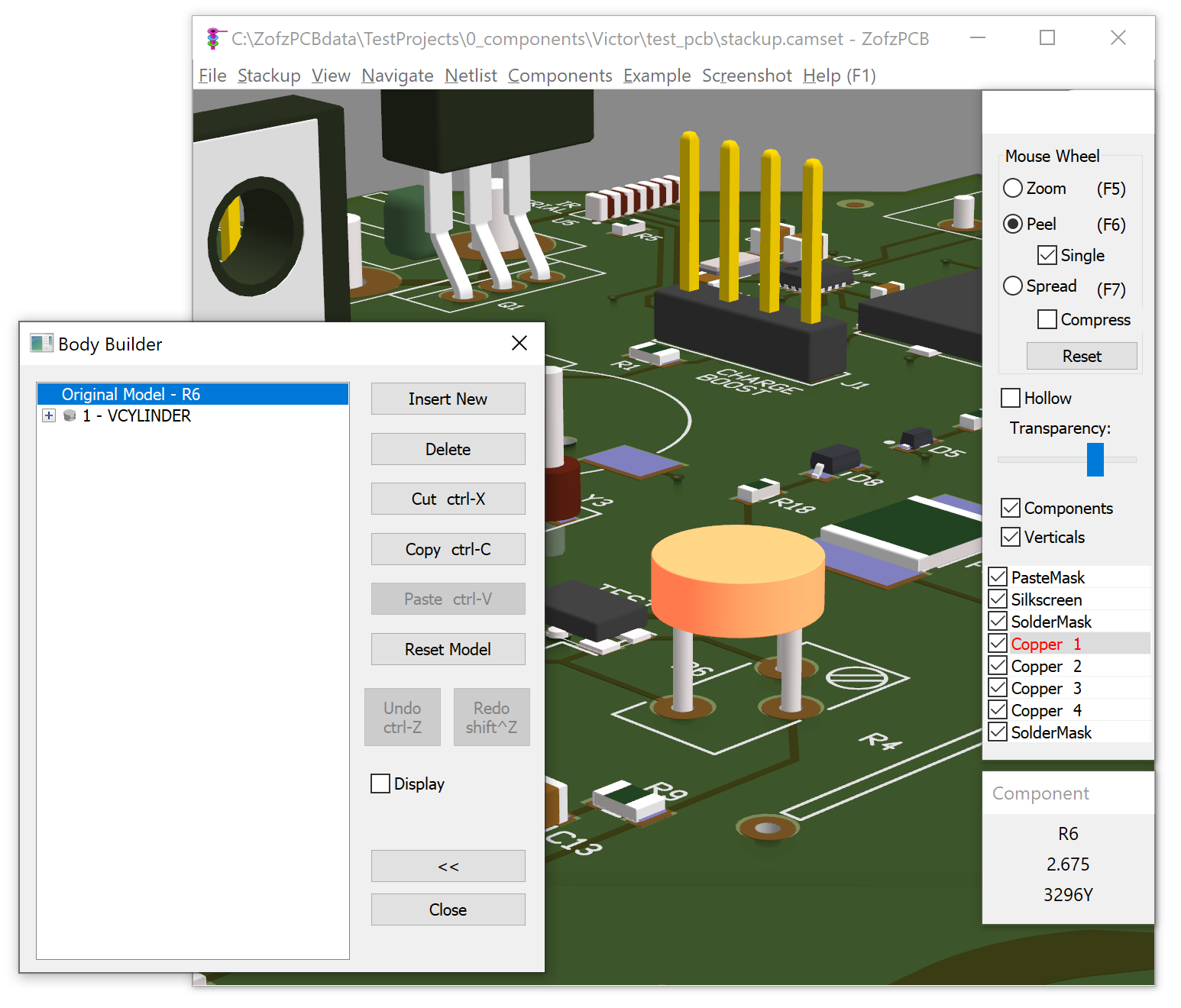
-
There is a list of graphical objects (primitives) on the left and tool buttons on the right.
List of the Body Primitives:- Tree View with plus-boxes. You can unroll the content of the primitive to gain access to the parameters.
- The selected primitive is highlighted (magenta). (*bug in version 2.0.1.0- it is not)
- Entering parameters one-by-one: use enter to accept and move to the following line.
- Insert New - show a list of primitives to insert
- Delete - remove the selected primitive(s)
- Cut - cut and store into the clipboard the selected primitive(s)
- Copy - store into the clipboard the selected primitive(s)
- Paste - insert the primitive(s) from the clipboard to the component in front of the selection
- Reset Model - clear the body and reload the Modeler created content
- Undo, Redo - there is a separate redo buffer for each component. This function works only for the Body Builder
- Display - only the edited component will be shown
- Return to the Modeler (in Component List): << button
- Close the Body Builder and the Modeler X or Close button
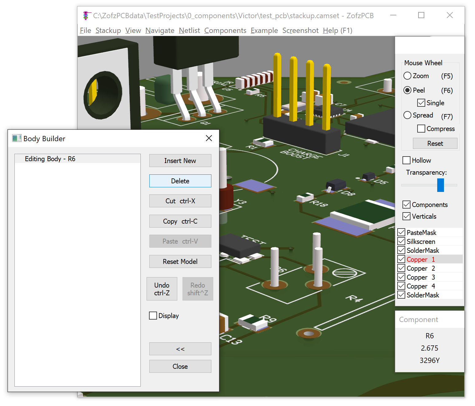
-
Next step: clear the body by selecting the current primitive (VCYLINDER) and pressing the
Delete button:
-
Next Step: Add one CUBE primitive by pressing the Insert New button and selecting the first item on the pop-up image list.
-
Next Step: Fill in the sizes, positions, and colors, using x,y,z dimensions from the variable resistor technical drawing (pdf).
Set all the rounded edges (RadHor, RadVert, RadLat) to 0.1mm and the distance from the PCB (h0) to 0.05mm. Get the color value from the element picture using the color picker tool (Drag & drop pipette).
Calculate the shift distance between the component origin (center between two external pins, in case of 3 pin devices) and the center of the CUBE primitive. Use paper, pen, and calculator. (sorry)
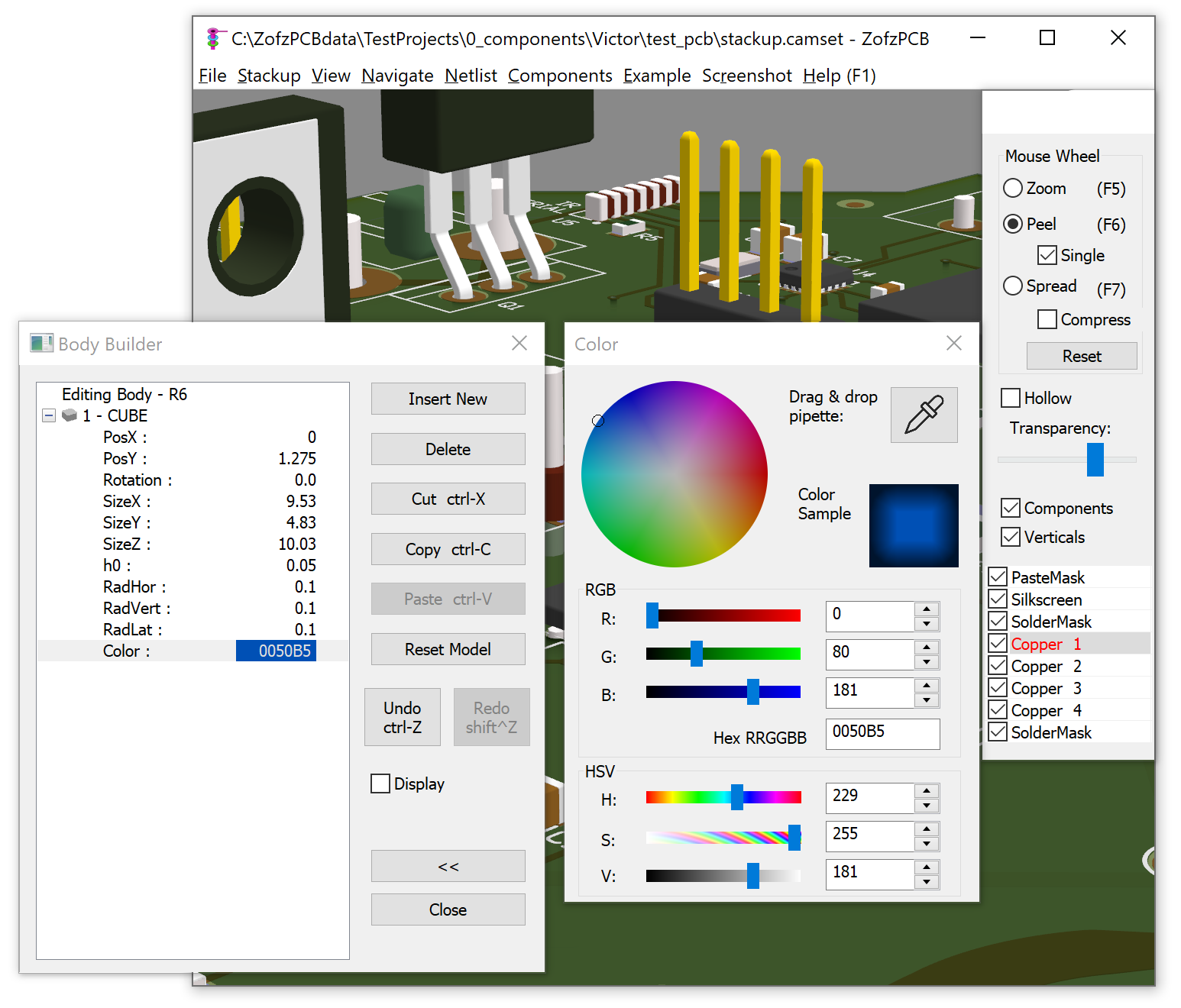
The result:
-
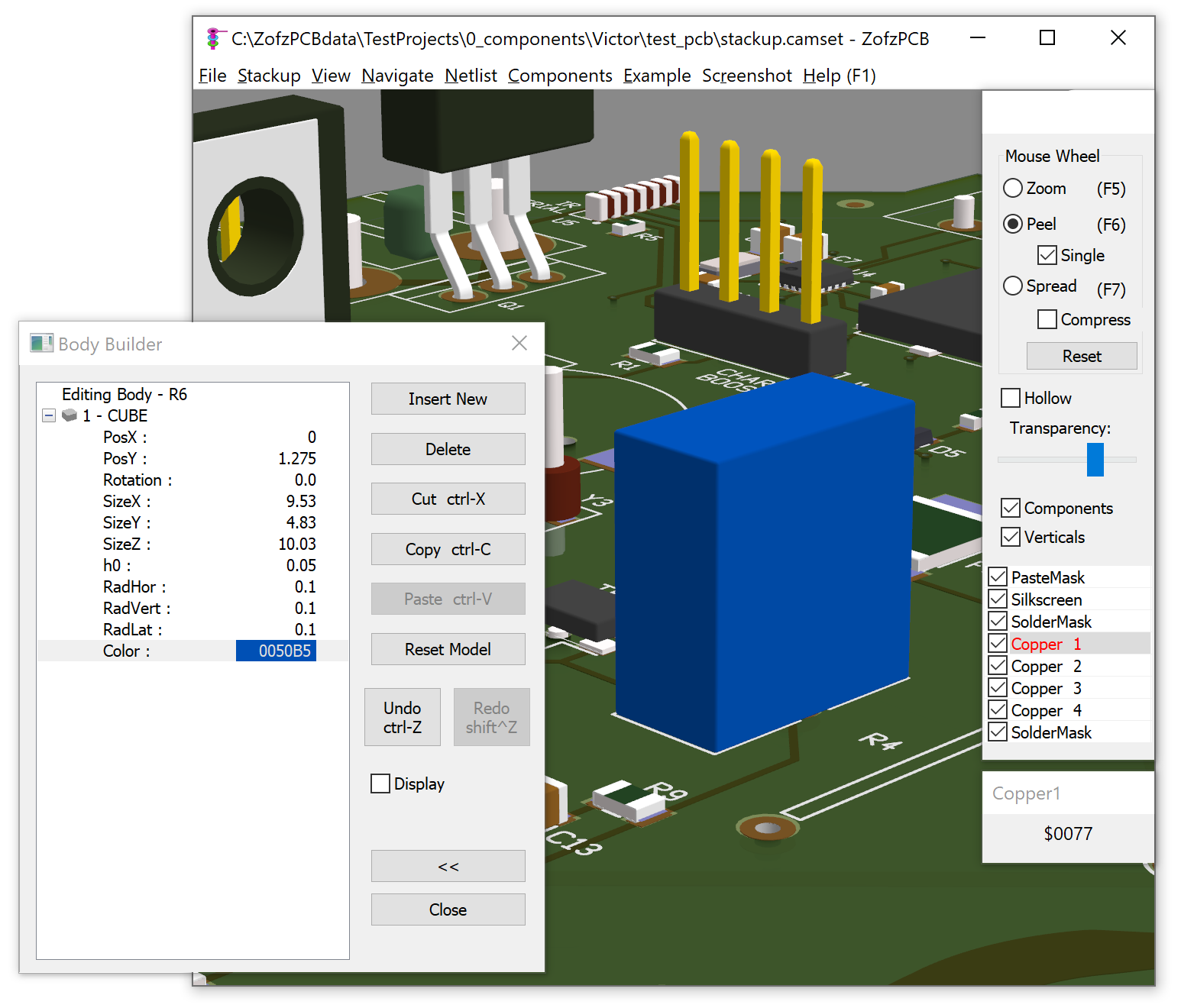
Next Step: As it would be impossible to construct the screw head with the slot out of currently
supported primitives, I have decided to elaborate more on the body instead and build it from 3 cubes,
gaining the sticking-out sides.
Shrink the SizeX to 0.6mm. Then calculate the required shift (PosX), so the external wall keeps to the component size. Then duplicate the primitive using clipboard and flip one wall to the other side, adding a minus sign to its PosX.
-
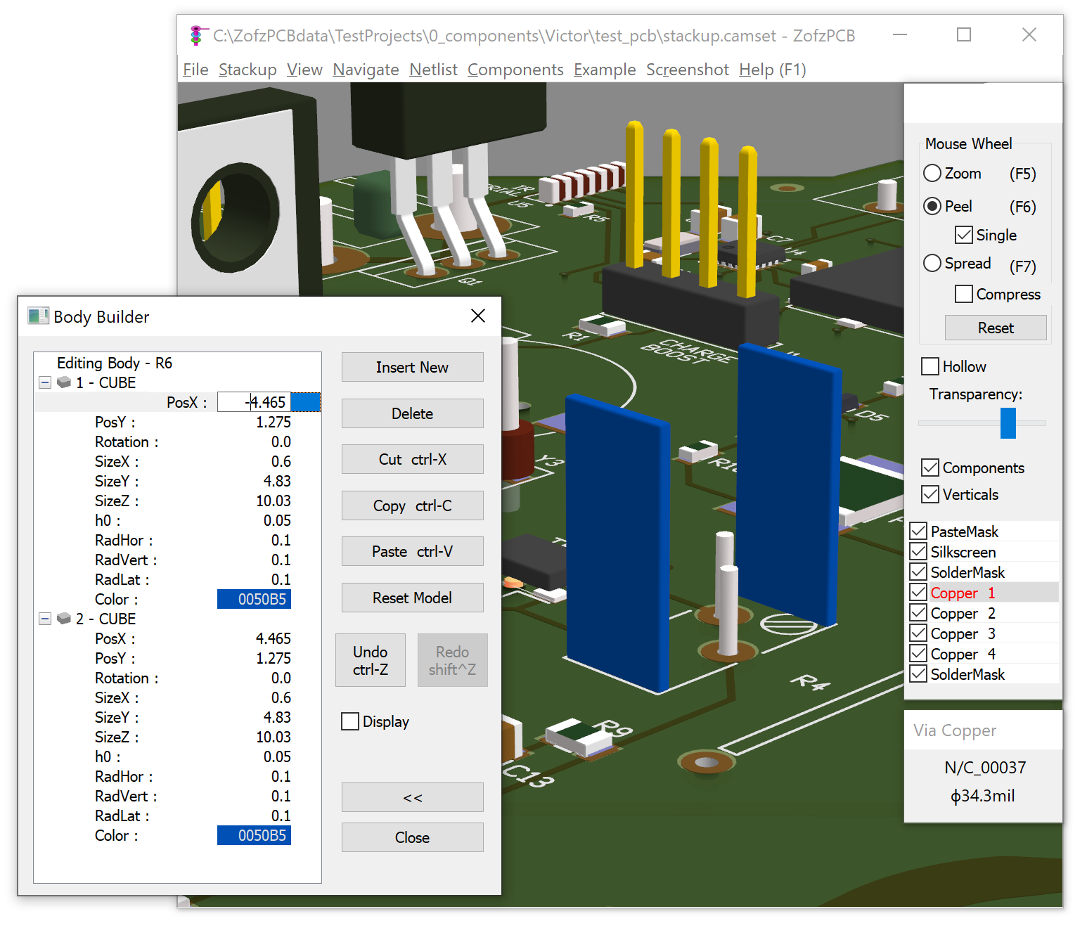
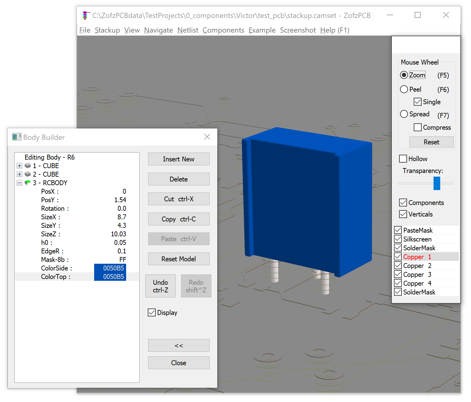
Next Step: The third cube primitive, between the two walls, can save some of the surfaces for faster rendering.
Consider using the RCBODY primitive. The RCBODY originally is used in the chip resistor or capacitor model.
Two surfaces of it are not drawn, as the terminals cover it. It also has two colors, as the chip resistor
has a different material on top. Additionally, all of its eight surfaces can be disabled by a mask bit-field.
In this case, the SizeX of the primitive must be longer than it is calculated to cover the edge radius of the two walls. So add even more 0.01mm to ensure it goes into contact with the walls.
The rotation is 0, so the two open sides go together with the already made walls. The SizeY is now smaller, by 0.53mm, to expose the edges of the walls. Also, the position PosY must be increased by 0.53mm/2 to align one of the sides and leave the whole 0.53mm on the other side.
Set both colors to a copy of the wall colors.
Please use the Display Checkbox to enable the single component view:
-
Next Step: The screw is made of a vertical cylinder, using VCYLINDER primitive, originally used for electrolytic capacitor.
As the primitive is hidden inside the already made body, set the height (h0) to move it above the body:
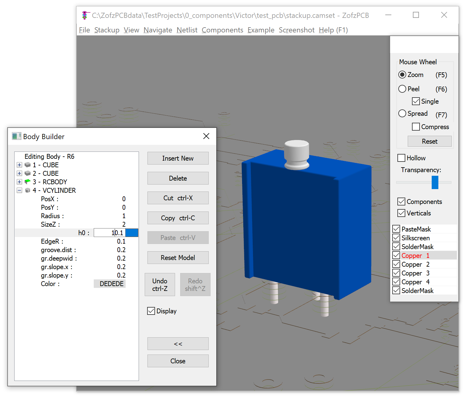
- Next Step: Disable the el-cap grove, by setting the grove parameters to 0, set the Radius and SizeZ to match
the data from the part drawing. You may submerge the screw a bit. Set the screw position.
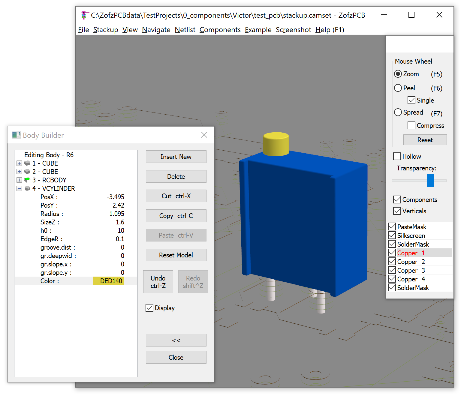 The Variable Resistor Body is now finished.
- Version 2.0.1.0 note: Uncheck the Display box before closing the Body Builder dialog. Due to a bug, this will not happen automatically, and the program will have disabled the whole board display.
-
If you have more than one part instance, use the Modeler global change buttons seen in the first picture.
The second option is to use the clipboard to copy the body into the body of the other components.
Using the clipboard, you can also copy the body element between different projects.
YouTube: body builder (old UI)
YouTube: Reuse component from another design (old UI)
4. STEP File Export
ZofzPCB STEP export feature makes use of facilities provided by the Open CASCADE Technology software.
How to create a STEP file?
- Load gerber files to ZofzPCB
- Check the 3d view, adjust component models
- Hide components you want to substitute own models for
- Menu: Files / STEP Export
- File Explorer "Save As" dialog shows up.
- Select the export Mode:
- Mechanical
You can specify objects to export using dedicated checkboxes. In the case of multilayer PCB, all internal layers are merged into one core. (Or two cores, in case of blind vias.) The Mechanical Mode lets you export any combination of the external PCB layers and components. Object colors are preselected. - Thermal Solver
The program will export everything in detail—even the metalization of drills and internal layers, grouped one by one. Object colors are taken from the PCB colors setup.
There are two suboptions, to select Layers To Export:- As Selected
The program will export layers enabled in the main view (side panel check-box). You may disable the export of the Cores by moving the Transparency slider to the leftmost position. - All
The program will simply export all layers and cores.
- As Selected
- Electromagnetic Field Solver
As above, except objects are grouped by nets. This lets you analyze only relevant nets. All conductive layers are always exported. You can enable or disable the export of dielectric layers, as in the above mode.
Elements are not overlapping. Metalized drill barrels are segmented when connected to internal layers.
- Mechanical
- Choose STEP file path and press the STEP Export button.
STEP Save As Dialog - Mechanical Mode:

STEP Save As Dialog - Thermal Solver Mode:

See Also:
More information can be found on ECAD/MCAD Collaboration - STEP file export
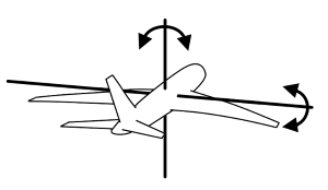
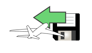
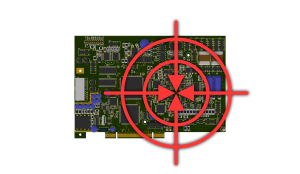
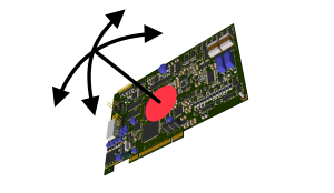
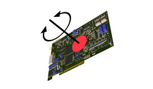
5. Navigation
The navigation process requires a wheel mouse and a keyboard. In addition, the ZofzPCB program supports 3Dconnexion 3D mouse.
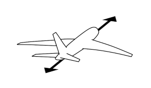
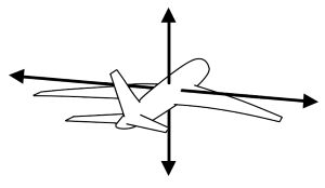
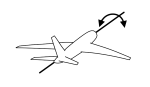
To illustrate how navigation is done using the wheel mouse and keyboard, an airplane has been used to represent different viewpoints.
In the following illustrations, the function of every key is given together with a corresponding viewpoint.
| F1 | quick keyboard help | 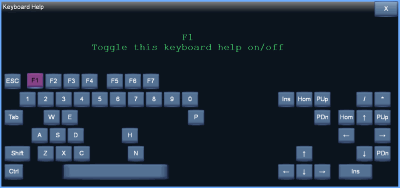 |
| PgUp-PgDn | CAM forward - backward |
 |
|
Up-Down, Left-Right |
CAM shift / hover |
 |
|
Numeric pad / * Ctrl- / * |
CAM roll, Ctrl=next rectangular |
 |
| A-D, S-W | CAM pan, tilt |
 |
| Right Mouse Button DRAG | CAM pan - tilt |
|
| Tab | roll to level the floor |
 |
| Space Bar | nearest rectangular |
 |
|
Home Ctrl-Home |
initial position |
 |
| Alt-Home |
resize PCB to fit in orthogonal projection |
 |
| Z | swap side |
 |
| X | turn to PCB center |
 |
|
Ctrl-1 ... Ctrl-9, Ctrl-0 |
Save current camera position |
 |
| 1 ... 9, 0 | Jump to saved camera position |
 |
| Left Mouse Button CLICK | center this PCB point |
 |
| Left Mouse Button DRAG | rotate around this PCB point |
 |
| Ctrl - Left Mouse Button DRAG | rotate around this PCB point |
 |
6. Right Panel: Layers & effects
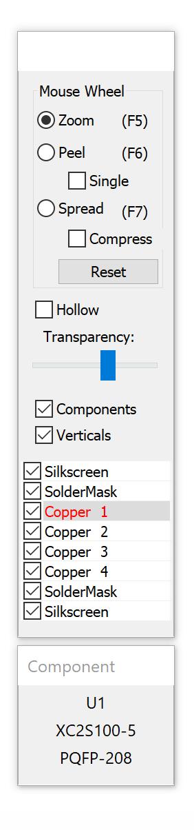
Zofzpcb offers fast access options on its right side panel. The following are the available options:
- Mouse wheel functions:
- Zoom (F5): mouse wheel is used for navigation (camera forward-backward)
- Peel (F6): removes layers one by one from the actual PCB top (or bottom if the camera is under the board).
Checkbox "Single" - check to view a single layer only. - Spread (F7): magnifies the z-axis of the PCB, thereby spreading all layers and drills proportionally.
Checkbox Compress - check to spread only the core and keep coper e.t.c. on initial thickness. - Reset Button - reset the position of the layers.
- Hollow Checkbox: makes continuous fields of layers transparent. This mode allows unobstructed view thru the ground/power planes.
- Transparency Slider: increase core/prepreg volume opacity.
The leftmost position of the slider enables a view of components on the other side of the PCB. - Components Checkbox: enable or disables component display.
- Verticals Checkbox: enable or disables vias, drill, and board edges display.
- On-Off layer checkboxes: activates or inactivates the selected layers.
(Click on the checkbox rectangle, not the layer name.) - Click on Layer name – turns on the single layer (Peel) mode for the selected layer.
(Now you can use the mouse wheel to change the layer.) - The visible (topmost) copper layer is marked by red color in the On/Off checkbox.
- In addition to the above options, the additional window below displays mouse-hover and selected object information.
The information about the selected object overwrites the hover display if you use the Pin-List Dialog or the Netlist Dialog.
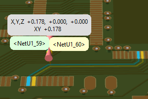
7. Measurements
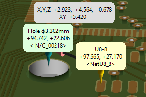
In a 3D arrangement, setting end-points is not that clear as on a 2D surface. Therefore you can set the end-point markers at a specific locations:
- Hole center.
- Pad center.
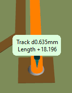
- Edge of a track or any other shape - you have a possibility to adjust the position, but the marker must stay on the edge. You start the selection by pointing to the shape and then, you can drag the marker, even moving the mouse pointer outside the shape.
- Track center - selecting track center highlights the whole track.
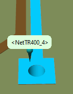
- Net - selecting the net highlights the whole net. This might be spreading to other layers. You have a possibility to select the visualisation method. See: Net-Marker by pressing ^N or Menu: View / Net Selection Effect
- ESC – reset markers
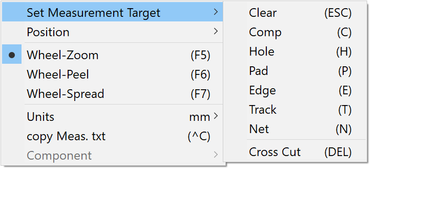
Zofzpcb offers some keys as additional mouse buttons. The keys used for this function are H, P, E, T, N (and <Del> for the Cross Section Cut). You can utilize their assigned functions either by using the keyboard or by selecting Right-Click Menu: Set Measurement Target.
7.1 Selections of measurements
Selecting an object will stay the same, but the distance marker may be automatically adjusted for the shortest distance, for example, a track and a hole - automatically changing the position of the marker along the track.
If you select more than two markers, the first one will remain in its place, while the second will follow your next selections. The first one, colored green, is the reference position. The program allows you to place the first marker again by clicking the object key twice in the same place or resetting the markers (using the ESC key).
You can keep the keys down to search for the object and set the marker continuously. This feature is handy for the E-edge key.
In addition, you can copy the dimensions text to the clipboard by pressing Ctrl-C
The table below shows what measurement the program will execute for the case of a different
combination of the measurement points.
Please hover your mouse cursor over the table...
| Hole | Pad | Edge | Track | Net | |||||||||||||||||||||
|---|---|---|---|---|---|---|---|---|---|---|---|---|---|---|---|---|---|---|---|---|---|---|---|---|---|
 |
 |
 |
 |
 |
|||||||||||||||||||||
| Hole | Pad | Edge | Track | Net | |||||||||||||||||||||
| Hole | 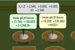 Distance
|
 Distance
|
 Distance
|
 Minimum Distance
|
 Minimum Gap Length
|
||||||||||||||||||||
| Pad |
Distance
|
 Distance
|
 Gap @ edge-point
|
 Minimum Distance
|
 Minimum Gap Length
|
||||||||||||||||||||
| Edge |
Distance
|
Gap @ edge-point
|
 Distance
|
 Minimum Distance
|
 Gap @ edge-point
|
||||||||||||||||||||
| Track |
Minimum Distance
|
Minimum Distance
|
Minimum Distance
|
 Minimum Distance
|
 Minimum Distance
|
||||||||||||||||||||
| Net |
Minimum Gap Length
|
Minimum Gap Length
|
Gap @ edge-point
|
Minimum Distance
|
 Minimum Gap Length
|
||||||||||||||||||||
| Hole | Pad | Edge | Track | Net |
YouTube: Explanation of measurements
7.2 Net-Marker
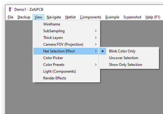
The program allows you to adjust the way you view your net selection. To switch the mode, please go to View and select Net Selection Effect or press Ctrl-N to circulate via available options. The available options are: blink color only, uncover selection, and show only selection.
 |
 |
 |
| Blink Color Only | Uncover Selection | Show Only Selection |
7.3 Text balloons
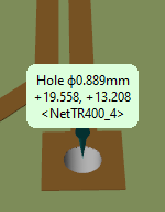
Three text balloons are possible: two marker balloons and one distance balloon. The balloons disappear when the mouse pointer gets near it to allow you subsequent selections or other mouse actions.
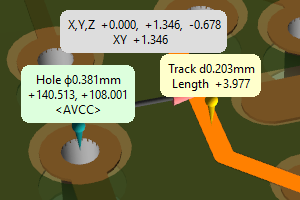
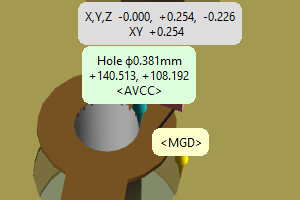
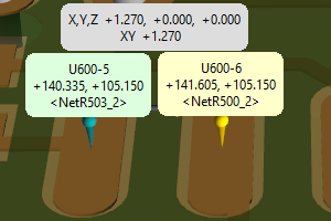
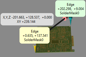
The distance balloon shows three axis X, Y, and Z distance, and the distance projected to the XY-pane.
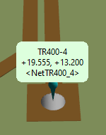
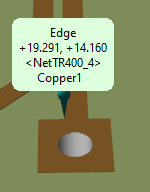
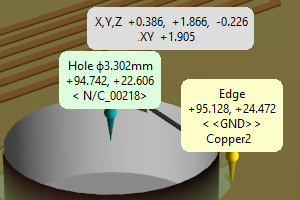
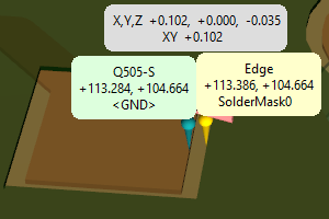
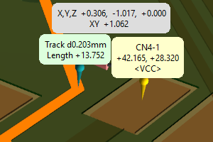
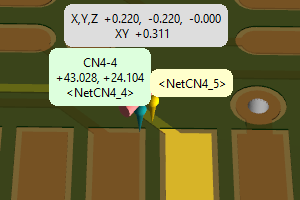
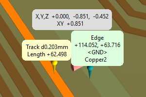
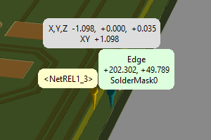
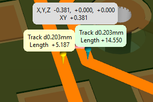
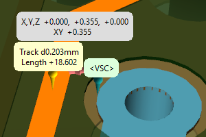
The marker balloon shows the type of the marker and information related to it:
- Hole
hole diameter, center XY position, Net-Name. - Pad
Component refID-pin-name, actual XY position, Net-Name. - Edge
XY position, Net-Name, Layer Name. - Track
Width, Length. - Net
Net Name
8 Right-Mouse-Button click menu
Clicking the right mouse button allows you to do the following:
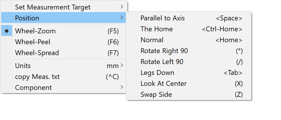
- Go to measurements functions without using the keyboard. (Set Measurement Target)
- Set Predefined position of the camera without using the keyboard.
- Access Mouse Wheel function switch. (The same as on the Right-Panel)
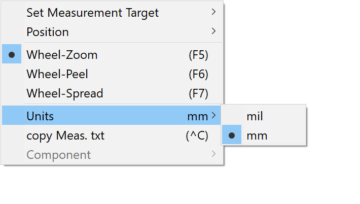
- Select mils or millimeters for measurement display.
- Copy the measurement text to clipboard. (^C)
- If called on a component:
See: Components and IPC-356 file and Components Modeler
- Hide the component.
- Flip the component placement side - top/bottom. (THT components)
- Evoke Modeler pop-up. See: Components Modeler
- If called on a disabled component(s) - show a list of components to unhide.
9. Cross Section
A perpendicular cross-section surface can be placed with and without the help of distance (measurement) markers.
If the markers are not set, the board tilt determines the starting direction and side of the cut surface, created at the mouse pointer position. The open (visible) side of the cut surface is always facing the camera. Note that the starting orientation is not determined if the PCB is in a home (perpendicular) position.
The action is started by pressing and holding the <Del> key. Dragging the mouse with the <Del> key pushed allows selecting the direction of the cut surface. Circulate the mouse pointer around the rotation center. The angle jumps every 45°. To adjust the angle in a free way, press the <Shift> key. When you are done setting the angle, release the <Del> key. Until the cut surface is removed, any mouse movement with the <Del> key pressed shifts the cut surface without rotating it.
You can achieve the same action via mouse operation only by using right-click menu: Set Measurement Target / Cross Cut. See the following video for an example of this action.
When a single distance marker is placed, the cut line is defined by the marker and the mouse pointer. It is still possible to adjust the line direction by keeping the <Del> key down and moving the mouse.
If two distance markers are present, the cut line is defined by the markers and a single press of the <Del> key.
10. View Menu - still some more effects
View Settings are usually related to GPU performance tuning, as with other Direct3D programs, such as 3D games.
If you encounter a low frame rate, consider reducing the GPU load by reducing details.
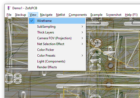
- Wireframe – this mode displays surfaces as frames of wires. Apart from helping in debugging,
this setting enables the user to quickly understand how the program carries out the flattening and triangulation process.
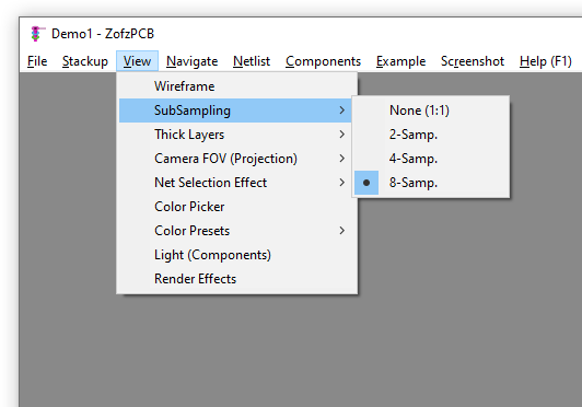
- SubSampling – increasing the sub-sampling enhances the image quality, but doing so demands more resources.
The available options depend on your GPU capacity.
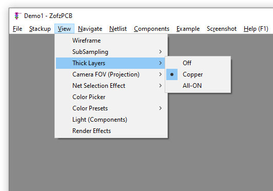
- Thick layers - thick layers are good-looking if your GPU can render them fast.
It is important to note that showing the thickness of copper, silkscreen, or solder mask layers can affect the frame rate significantly. There are more triangles in the edges than in the front surfaces!
- Camera FOV
Model 3D → screen 2D Projection Settings
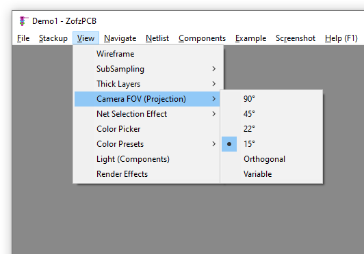
Camera FOV (Field Of View) is equivalent to adjusting a focal length of the camera lenses. There are the following settings:
- 4 presets 90°, 45°, 22.5°, 15°.
Note: the 90° setting (and square display proportions) is crucial in building the 360°x180° panorama pictures, if you ever wish to create it. - Orthogonal
The orthogonal mode is based on a simple projection and does not feature a perspective effect.
If you keep camera direction perpendicular to the PCB, by using Home or space-bar buttons, there will be a specific size scale relating the PCB and the viewed image.
This scale value is saved in the Screenshot image meta data to allow for 1:1 printing. - Variable: a pop-up containing a scroll-bar shows up.
An Additional effect, Compensate / Dolly Zoom, moves the camera forward and backward thereby allowing compensation of the object’s size change.
- 4 presets 90°, 45°, 22.5°, 15°.
- Net selection effects (see: Net-Marker)
- Color Presets
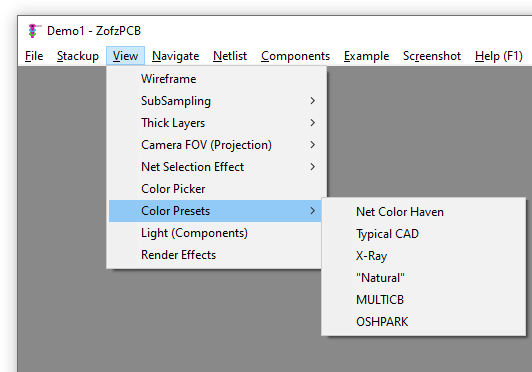
Besides the predefined options, the program allows you to create and save your own color presets.
Presets are stored in "%appdata%\ZofzPCB\NAME.color" folder. The path is given to enable you to copy, share, or distribute your color presets. You can save any current color settings, as a Color Preset, in the Color Picker Dialog, see below... - Color Picker
To access the color picker, please go to Menu/View and select "Color Picker".
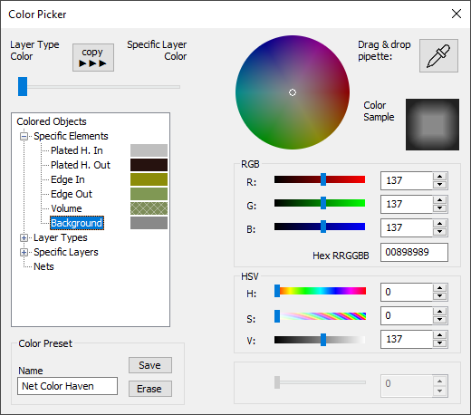
Top Slider:
There are two color tables: one for layer type and the other for individual layers.
The slider at the top allows the mixing of the colors from both tables in proportion.
Please select the related entry in the Tree View to modify a color from the specific table.Tree View ("Colored Objects") lists four root branches: Specific Elements, Layer Types, Specific Layers, and Nets.
- Specific Elements - holes, edges, volume (Core), background.
- Layer Types - Paste Mask, Silkscreen, Copper, etc., related by type. This branch represents real life (material-dependent) coloring scheme.
- Specific Layers - as in the current stackup. Each layer from top to bottom. This branch represents a coloring scheme like in a 2D CAD.
- Nets - manual color overwrites to specific nets. This branch is empty by default.
After selecting the specific object in the "Colored Objects" Tree View, the object's color can be adjusted using controls on the right side of the dialog.
From top to bottom:- Clicking or dragging on the chroma wheel
- RGB sliders (and numerical values)
- HSV sliders (and numerical values)
- HEX RRGGBB numerical value
- Drag & drop pipette
Some objects have an additional color feature: Opacity or the Net-Color, adjustable by the right bottom slider.
Opacity: for example PCB Core or Solder Mask,
Net Color: copper elements may be colored by a symbolic net-color, allowing for easy tracking of the copper connections.
The Net Color is a pseudo-random color selected for each detected net. When adjusting color of the conductive objects, you can mix the declared color with the random net color, using the bottom-right slider.The program allows overwriting the specific net color by positioning the mouse pointer over the particular track (on the PCB) and pressing the N-Net key.
The overwritten net names will appear under the Net branch in the Tree-View.It is possible to change all the net color random values "Set All Net Colors" are:
to Random pseudo random to This to the current net color to Copper to the Layer Type defined color - Light
To access the Component Models Lighting Options Dialog, please go to Menu / View and select "Light".
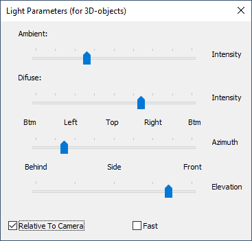
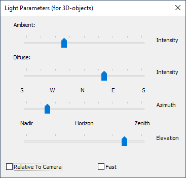
The program offers 2 types of lighting: Ambient and Diffuse. (The Specular light and textures are not implemented yet.)
Two images shows the dialog box in two modes: Left - Relative to Camera direction, Right - Absolute.
The controls:- Amount of the Ambient light (equivalent to offset, in electronic terms).
- Amount of Diffuse light
- Diffuse light direction: Azimuth
- Diffuse light direction: Elevation
- Diffuse light direction: Relative To Camera
The view is more uniform if the light direction is binded to the camera/navigation. Labels on the above 2 sliders change accordingly - Diffuse light direction: Fast
How fast the light follows the camera
- Render Effects
To access the Render Effects Parameters Dialog, please go to Menu / View and select "Render Effects".
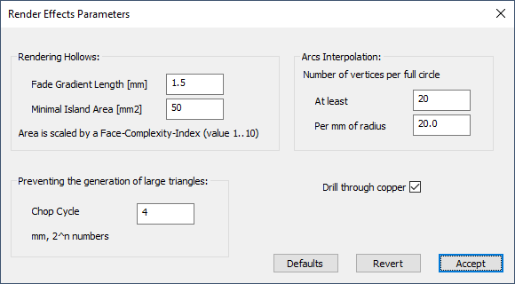
This is a set of parameters that change visual features. They are used during the triangulation phase. Note that the new values will have an effect after the next flattening and triangulation.- Rendering Hollows:
Refers to the thickness of the strip on which the smooth disappearance of the edge contour occurs.
A copper island cannot be rendered hollow if its area is smaller than the specified size.
In addition, the island must have a simple shape. For complex islands, a larger area is required to produce a hollowing effect. - Preventing the generation of large triangles:
Big (long) triangles can interfere with some visual features. The lighting and colors are calculated per vertex and are interpolated along the triangle edges. The density of this calculation should be high enough but also not take too much GPU resources.
Use numbers such as 1,2,4,8,16.. or 0.5, 0.25, 0.125. - Rendering Arcs to Polygons:
After the flattening process, arcs are converted into straight-line polygons. How exactly would you like to have it?
Netlist and hit tests are performed on data stored before the flattening process to ensure measurement accuracy. - Drill through copper
Should drills make holes in copper? Yes. But sometimes, it is helpful to skip this operation.
This setting affects triangulation and flattening.
- Rendering Hollows:
11. Screenshot
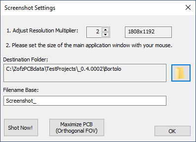
- This feature saves the current view in PNG format - lossless image compression format.
- The user interface elements are removed from the picture.
- The Resolution Multiplier allows you to upscale the resolution up to 10 times.
- You can resize the main window while the dialog is open. The dialog will display new resolution values.
- The program adds the current project folder to the "List Of Places" - left pane of the "Select Folder" dialog.
- The program generates unique filenames when saving.
- The program sets the Physical Dimension (DPI) in the pdf file when the camera is set to the orthogonal mode.
You can print out a 1:1 paper model of the PC (Ref 7.5)
Please use printing programs with honors DPI settings such as standard paint. - Maximize PCB (Orthogonal FOV) button, sets the magnification, so the PCB fits exactly to the image borders. (Only in the orthogonal mode.)
12. Autopilot
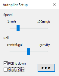
The autopilot offers automatically generated airplane-like camera movements. It is based on the PCB drills and provides the following:
- Speed scrollbar.
Besides short moments of slowdown when flying through the drills, the camera keeps a constant linear speed that is set using the scrollbar. - Roll scrollbar.
It sets the camera roll, thereby defining the bottom of the screen. The program offers two options:- Centrifugal- the down direction is perpendicular to the turning axis.
- Gravity- the down direction is perpendicular to the PCB plane.
- PCB is down.
When checked, the direction of gravity is towards the PCB. Otherwise, the direction is always from top to bottom. - Viaska City.
Enables peeling of all sections except the actual bottom layer of your PCB. - ➧➧➧ button
Starts or stops the action.
Enjoy a flight over your PCB with the autopilot!
13. Connection between Program and Website
The following is mostly located under menu: F1-Help
On-demand, start the Default Browser, directing it to:
- www.zofzPCB.com
- "User Manual" www.zofzPCB.com/help (this file)
- "User's Forum" www.zofzPCB.com/forum
- "FAQ Page" page www.zofzPCB.com/FAQ
- Example / Show Galery - displays www.pcbmodel.com website.
Send a Bug Report
This command starts an external program that allows you to send your message and log file. The log file is located at %APPDATA%\ZofzPCB\ZofzDebugLogFile.txt.
You can revise the log file before sending it. If you expect feedback from me, please provide your email address.
No other information is sent apart from what you can clearly see in the CrashReport.exe dialog window.Check for upgrade
Manually triggers the action described below:Automatic version check
When the program starts, the 3D Gerber Viewer automatically requests to check for the latest version every couple of days. This request is to be confirmed by the user. There are three options:
- Allow it
- Allow it forever
- Disallow it this time
The program compares the received version number to its version number - you will get the information about the new version when it is available. You can still defer or ignore the download or start it automatically via the default internet browser.
14. Bug Reports
Do not hesitate to send me a bug report.
I must reproduce the bug at my debugging workbench to debug the program.
If the bug is related to the input data, I need to ask you to provide me with the input data.
I understand the delicacy of the subject - I am designing PCBs myself.
So, reduce the Gerbers to the affected region and layers if you have time, or just trust me.
There is a link to the privacy policy.
Use bug@zofzpcb.com for direct contact.
List of known bugs, version log: bug list
"
15. Program Structure Chart
 Block diagram of the program (ver 1.1), showing data processing from CAD/CAM Gerber input to 3D Render Buffers.