Accurate Solder Mask 3D Model
Posted: Wed May 18, 2022 6:02 am
Is it possible to cover the solder mask layer topographically accurate on top of the copper layer ?
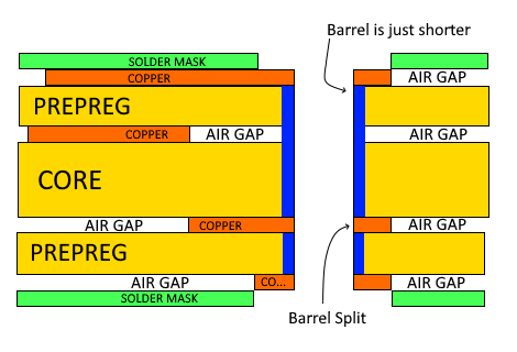
The current mask stack up has an air gap between solder mask an core, which is not real.
This would enable to simulate (using ANSYS HFSS) the impact of the solder mask layer, which is significant at higher frequencies > 5 GHz.
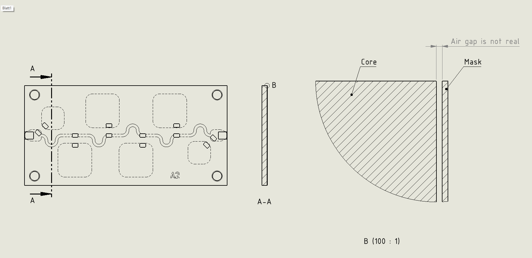
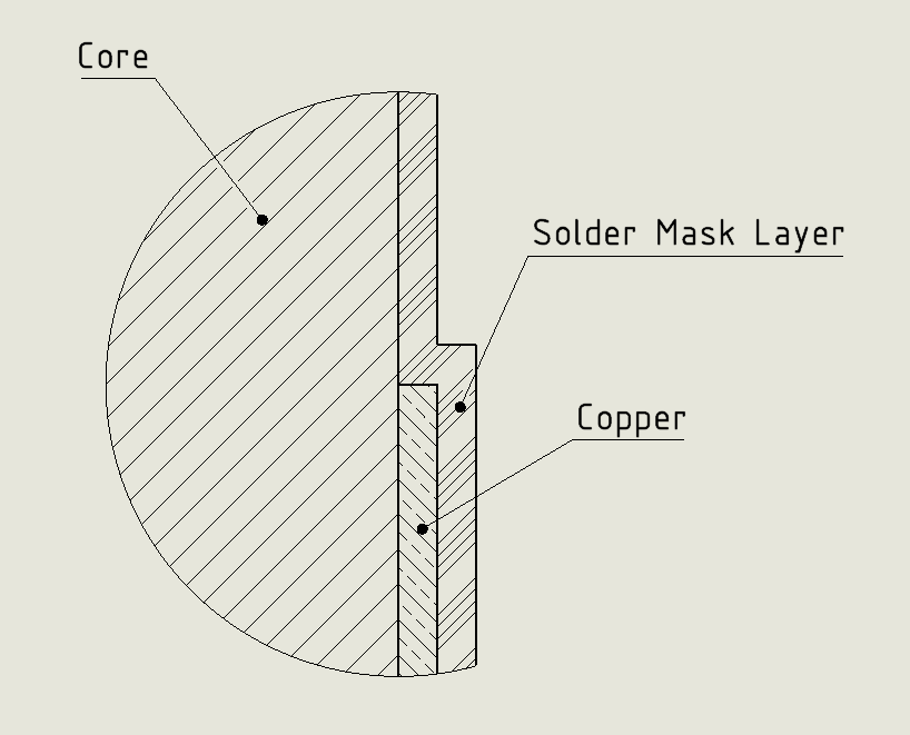
The current mask stack up has an air gap between solder mask an core, which is not real.
This would enable to simulate (using ANSYS HFSS) the impact of the solder mask layer, which is significant at higher frequencies > 5 GHz.