Yes, the concept of the layers is simple. Each layer has a defined Z-position and thickness.
And if it ever comes to the silkscreen layer, it will be even more gap.
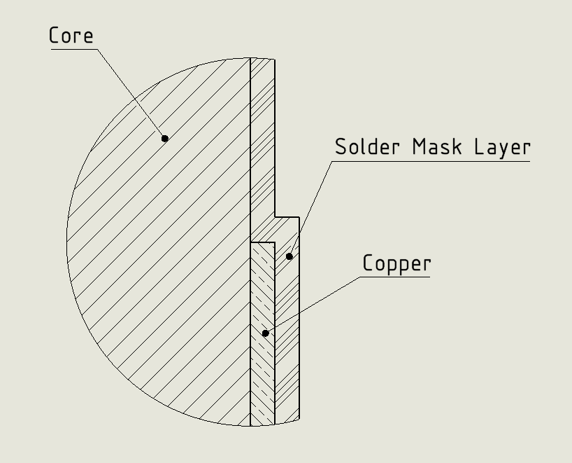
So, for the SolderMask, I would need to create two sub-layers:
- SolderMask AND NOT copper
- SolderMask AND enlarged-copper
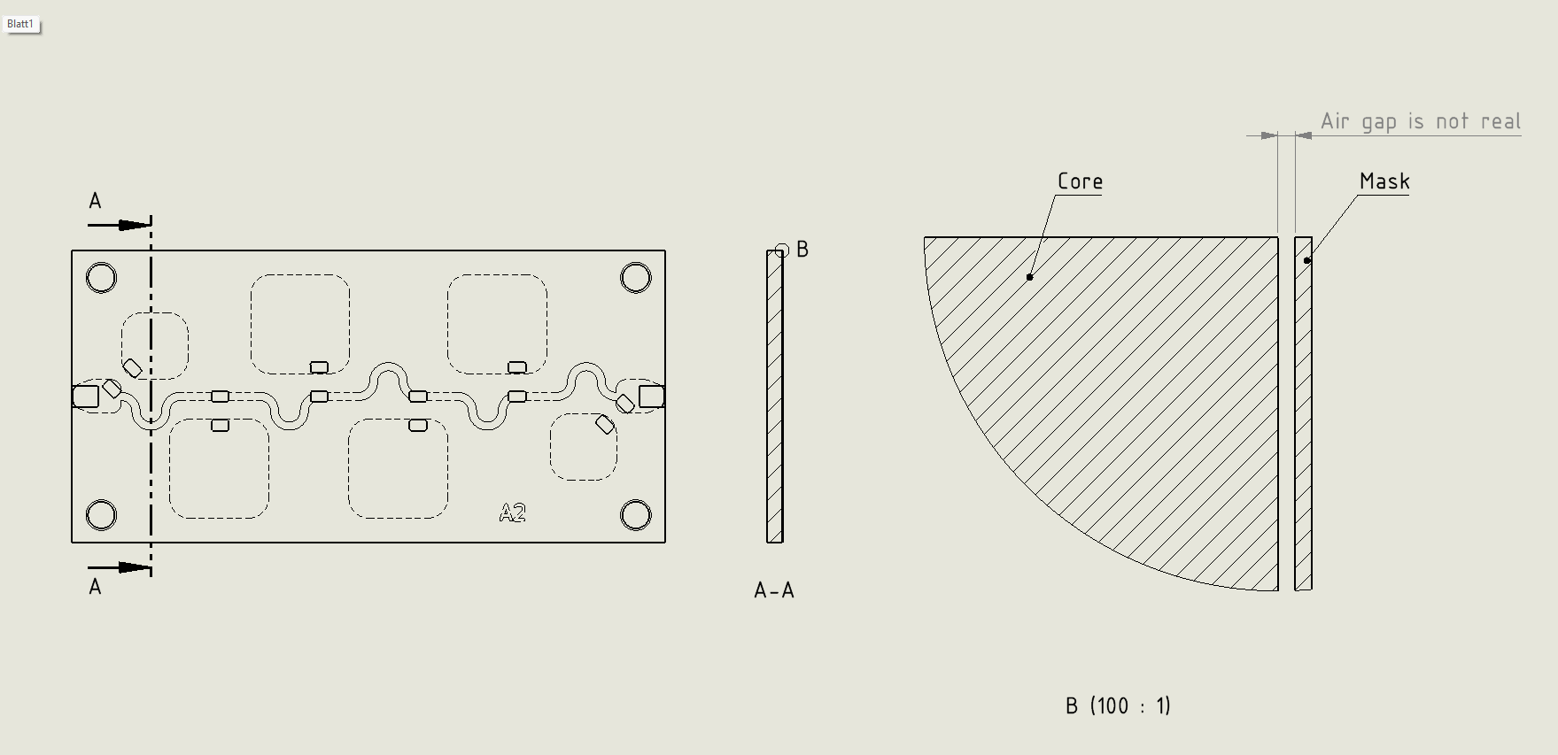
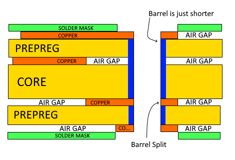
Also, the mid-layer air gap should be replaced by an extra core = BoardOutline AND NOT copper.
Now, the question is if this should be part of flattening, visible also in ZofzPCB native view, or only for the STEP export.
It also raises another question of a via tenting. That would be SolderMask AND NOT shrinked-drill.
Let me sort these things out in my mind.